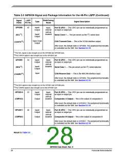
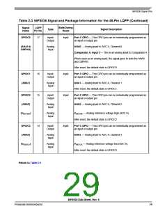
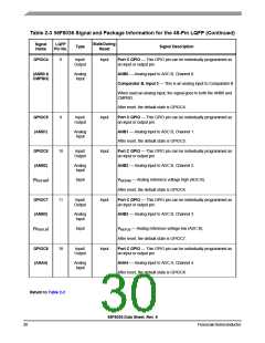
Table 2-3 56F8036 Signal and Package Information for the 48-Pin LQFP (Continued)
Signal
Name
LQFP
Pin No.
StateDuring
Reset
Type
Signal Description
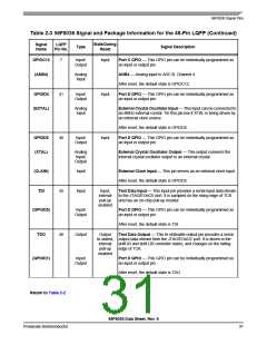
TCK
21
Input
Input,
internal
pull-up
enabled
Test Clock Input — This input pin provides a gated clock to
synchronize the test logic and shift serial data to the JTAG/EOnCE
port. The pin is connected internally to a pull-up resistor. A Schmitt
trigger input is used for noise immunity.
(GPIOD2)
Input/
Port D GPIO — This GPIO pin can be individually programmed as
Output
an input or output pin.
After reset, the default state is TCK.
TMS
47
Input
Input,
internal
pull-up
enabled
Test Mode Select Input — This input pin is used to sequence the
JTAG TAP controller’s state machine. It is sampled on the rising
edge of TCK and has an on-chip pull-up resistor.
(GPIOD3)
Input/
Port D GPIO — This GPIO pin can be individually programmed as
Output
an input or output pin.
After reset, the default state is TMS.
Note: Always tie the TMS pin to VDD through a 2.2K resistor.
Return to Table 2-2
56F8036 Data Sheet, Rev. 6
32
FreescaleSemiconductor

 FREESCALE [ Freescale ]