Introduction
Part 2 Signal/Connection Descriptions
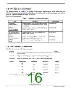
2.1 Introduction
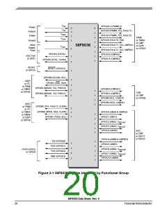
The input and output signals of the 56F8036 are organized into functional groups, as detailed in Table 2-1.
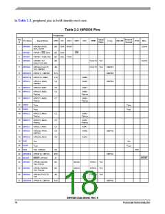
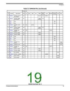
Table 2-2 summarizes all device pins. In Table 2-2, each table row describes the signal or signals present
on a pin, sorted by pin number.
Table 2-1 Functional Group Pin Allocations
Functional Group
Power Inputs (VDD, VDDA
Number of Pins
)
3
4
Ground (VSS, VSSA
Supply Capacitors
Reset1
)
2
1
Pulse Width Modulator (PWM) Ports1
Queued Serial Peripheral Interface (QSPI) Ports1
Timer Module A (TMRA) Ports1
12
4
4
Analog-to-Digital Converter (ADC) Ports1
Queued Serial Communications Interface 0 (QSCI0) Ports1
MSCAN Ports1
10
2
2
Inter-Integrated Circuit Interface (I2C) Ports1
Oscillator Signals1
2
2
JTAG/Enhanced On-Chip Emulation (EOnCE)1
4
1. Pins may be shared with other peripherals; see Table 2-2.
56F8036 Data Sheet, Rev. 6
Freescale Semiconductor
17

 FREESCALE [ Freescale ]