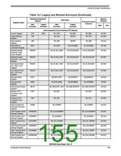
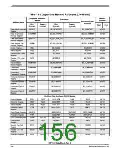
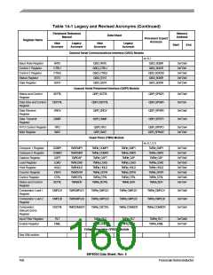
Table 14-1 Legacy and Revised Acronyms (Continued)
Peripheral Reference
Data Sheet
Memory
Address
Manual
Processor Expert
Register Name
Acronym
New
Legacy
New
Legacy
Start
End
Acronym
Acronym
Acronym
Acronym
Clear Activity Interrupt
Register
CLRACT
CLRSTPDET
CLRSTDET
CLRGC
I2C_CLRACTIVITY
I2C_CLR_STOPDET
I2C_CLR_STAR_DET
I2C_CLR_GENCALL
I2C_CLRACTIVITY
I2C_CLR_STOPDET
I2C_CLR_STAR_DET
I2C_CLR_GENCALL
0xF2AE
0xF2B0
0xF2B2
0xF2B4
Clear Stop Detect
Interrupt Register
Clear Start Detect
Interrupt Register
Clear General Call
Interrupt Register
Enable Register
Status Register
ENBL
STAT
I2C_ENABLE
I2C_STAT
I2C_ENABLE
I2C_STAT
0xF2B6
0xF2B8
0xF2BA
Transmit FIFO Level
Register
TXFLR
I2C_TXFLR
I2C_TXFLR
Receive FIFO Level
Register
RXFLR
I2C_RXFLR
I2C_TX_ABRTSRC
I2C_COMPARM1
I2C_COMPARM2
I2C_COMVER1
I2C_COMVER2
I2C_COMTYP1
I2C_COMTYP2
I2C_RXFLR
I2C_TX_ABRTSRC
I2C_COMPARM1
I2C_COMPARM2
I2C_COMVER1
I2C_COMVER2
I2C_COMTYP1
I2C_COMTYP2
0xF2BC
0xF2C0
0xF2FA
0xF2FB
0xF2FC
0xF2FD
0xF2FE
0xF2FF
Transmit Abort
Source Register
TXABRTSRC
COMPARM1
COMPARM2
COMVER1
COMVER2
COMTYP1
COMTYP2
Component
Parameter 1 Register
Component
Parameter 2 Register
Component Version 1
Register
Component Version 2
Register
Component Type 1
Register
Component Type 2
Register
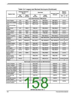
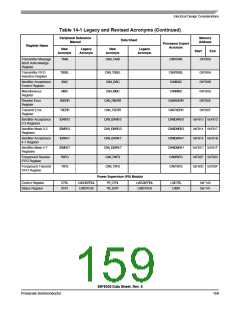
On-Clock Chip Synthesis (OCCS) Module
Control Register
Divide-By Register
Status Register
CTRL
DIVBY
STAT
PLLCR
PLLDB
PLLSR
OSCTL
OCCS_CTRL
OCCS_DIVBY
OCCS_STAT
OCCS_OCTRL
PLLCR
PLLDB
PLLSR
OSCTL
PLLCR
PLLDB
PLLSR
OSCTL
0xF130
0xF131
0xF132
0xF135
Oscillator Control
Register
OCTRL
Clock Check Register
Protection Register
Clock Divider Register
CLKCHK
PROT
OCCS_CLCHK
OCCS_PROT
FM_CLKDIV
FM_CNFG
PLLCLCHK
PLLPROT
FMCLKD
FMCR
OCCS_CLCHK
OCCS_PROT
FMCLKD
0xF136
0xF137
0xF400
0xF401
CLKDIV
CNFG
FMCLKD
FMCR
Configuration
Register
FMCR
Security High Half
Register
SECHI
SECLO
PROT
FMSECH
FMSECL
FMPROT
FM_SECHI
FM_SECLO
FM_PROT
FMSECH
FMSECL
FMPROT
FMSECH
FMSECL
FMPROT
0xF403
0xF404
0xF410
Security Low Half
Register
Protection Register
56F8036 Data Sheet, Rev. 6
156
FreescaleSemiconductor

 FREESCALE [ Freescale ]