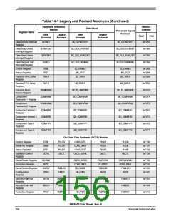
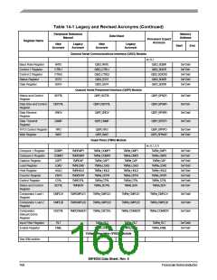
Table 14-1 Legacy and Revised Acronyms (Continued)
Peripheral Reference
Data Sheet
Memory
Address
Manual
Processor Expert
Acronym
Register Name
New
Legacy
New
Legacy
Acronym
Start
End
Acronym
Acronym
Acronym
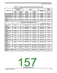
Queued Serial Communications Interface (QSCI) Module
n= 0, 1
Baud Rate Register
Control 1 Register
Control 2 Register
Status Register
RATE
CTRL1
CTRL2
STAT
QSCI_RATE
QSCI_CTRL1
QSCI_CTRL2
QSCI_STAT
QSCI_DATA
QSCI_SCIBR
QSCI_SCICR
QSCI_SCICR2
QSCI_SCISR
QSCI_SCIDR
0xF2n0
0xF2n1
0xF2n2
0xF2n3
0xF2n4
Data Register
DATA
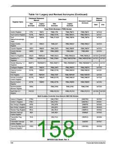
Queued Serial Peripheral Interface (QSPI) Module
Status and Control
Register
SCTRL
DSCTRL
DRCV
QSPI_SCTRL
QSPI_SPSCR
QSPI_SPDSR
QSPI_SPDRR
QSPI_SPDTR
0xF2n0
0xF2n1
0xF2n2
0xF2n3
Data Size and Control
Register
QSPI_DSCTRL
QSPI_DRCV
QSPI_DXMIT
Data Receive
Register
Data Transmit
Register
DXMIT
FIFO Control Register
Wait Register
FIFO
QSPI_FIFO
QSPI_WAIT
QSPI_SPFIFO
QSPI_SPWAIT
0xF2n4
0xF2n5
WAIT
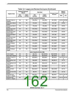
Quad-Timer (TMR) Module
n= 0, 1, 2, 3
Compare 1 Register
Compare 2 Register
Capture Register
Load Register
COMP1
COMP2
CAPT
TMRCMP1
TMRCMP2
TMRCAP
TMRn_COMP1
TMRn_COMP2
TMRn_CAPT
TMRn_LOAD
TMRn_HOLD
TMRn_CNTR
TMRn_CTRL
TMRn_SCTRL
TMRn_CMP1
TMRn_CMP2
TMRn_CAP
TMRn_LOAD
TMRn_HOLD
TMRn_CNTR
TMRn_CTRL
TMRn_SCR
TMRn_CMP1
TMRn_CMP2
TMRn_CAP
TMRn_LOAD
TMRn_HOLD
TMRn_CNTR
TMRn_CTRL
TMRn_SCR
0xF0n0
0xF0n1
0xF0n2
0xF0n3
0xF0n4
0xF0n5
0xF0n6
0xF0n7
LOAD
HOLD
CNTR
CTRL
TMRLOAD
TMRHOLD
TMRCNTR
TMRCTRL
TMRSCR
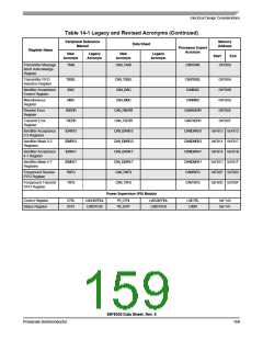
Hold Register
Counter Register
Control Register
Status and Control
Register
SCTRL
Comparator Load 1
Register
CMPLD1
CMPLD2
CSCTRL
TMRCMPLD1
TMRCMPLD2
TMRCOMSCR
TMRn_CMPLD1
TMRn_CMPLD2
TMRn_CSCTRL
TMRn_CMPLD1
TMRn_CMPLD2
TMRn_COMSCR
TMRn_CMPLD1
TMRn_CMPLD2
TMRn_COMSCR
0xF0n8
0xF0n9
0xF0nA
Comparator Load 2
Register
Comparator
Status/Control
Register
Input Filter Register
Enable Register
FILT
TMRn_FILT
TMRn_FILT
TMRn_FILT
0xF0nB
0xF0nF
ENBL
TMRn_ENBL
TMRn_ENBL
TMRn_ENBL
Voltage Regulator (VREG) Module
See SIM section
56F8036 Data Sheet, Rev. 6
160
FreescaleSemiconductor

 FREESCALE [ Freescale ]