General Characteristics
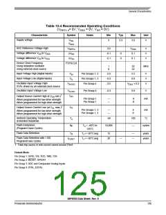
Table 10-4 Recommended Operating Conditions
(V = 0V, V = 0V, V = 0V)
REFL x
SSA
SS
Characteristic
Supply voltage
Symbol
Notes
Min
Typ
Max
Unit
VDD,
3
3.3
3.6
V
VDDA
ADC Reference Voltage High
Voltage difference VDD to VDDA
Voltage difference VSS to VSSA
VREFHx
ΔVDD
3.0
-0.1
-0.1
VDDA
0.1
V
V
V
0
0
ΔVSS
0.1
Device Clock Frequency
Using relaxation oscillator
Using external clock source
FSYSCLK
1
0
32
32
MHz
Input Voltage High (digital inputs)
Input Voltage Low (digital inputs)
Oscillator Input Voltage High
VIH
VIL
Pin Groups 1, 2
Pin Groups 1, 2
Pin Group 4
2.0
-0.3
2.0
5.5
0.8
V
V
V
VIHOSC
VDDA + 0.3
XTAL driven by an external clock source
Oscillator Input Voltage Low
VILOSC
IOH
Pin Group 4
-0.3
0.8
V
Output Source Current High at VOH min.)1
Pin Group 1
Pin Group 1
—
—
-4
-8
mA
When programmed for low drive strength
When programmed for high drive strength
Output Source Current Low (at VOL max.)1
IOL
Pin Groups 1, 2
Pin Groups 1, 2
—
—
4
8
mA
When programmed for low drive strength
When programmed for high drive strength
Ambient Operating Temperature
(Extended Industrial)
TA
NF
-40
105
—
°C
Flash Endurance
(Program Erase Cycles)
TA = -40°C to
125°C
10,000
cycles
Flash Data Retention
TR
TJ <= 85°C avg
TJ <= 85°C avg
15
20
—
—
years
years
Flash Data Retention with <100
Program/Erase Cycles
tFLRET
—
1. Total chip source or sink current cannot exceed 75mA
Default Mode
Pin Group 1: GPIO, TDI, TDO, TMS, TCK
Pin Group 2: RESET, GPIOA7
Pin Group 3: ADC and Comparator Analog Inputs
Pin Group 4: XTAL, EXTAL
56F8036 Data Sheet, Rev. 6
Freescale Semiconductor
125

 FREESCALE [ Freescale ]