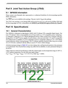
General Characteristics
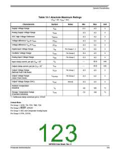
Table 10-1 Absolute Maximum Ratings
(VSS = 0V, VSSA = 0V)
Characteristic
Supply Voltage Range
Symbol
VDD
Notes
Min
-0.3
- 0.3
- 0.3
- 0.3
- 0.3
- 0.3
- 0.4
- 0.3
—
Max
4.0
Unit
V
Analog Supply Voltage Range
ADC High Voltage Reference
Voltage difference VDD to VDDA
Voltage difference VSS to VSSA
Digital Input Voltage Range
Oscillator Voltage Range
VDDA
VREFHx
ΔVDD
ΔVSS
VIN
4.0
V
4.0
V
0.3
V
0.3
V
Pin Groups 1, 2
Pin Group 4
6.0
V
VOSC
VINA
4.0
V
Analog Input Voltage Range
Pin Group 3
4.0
V
Input clamp current, per pin (VIN < 0)1
Output clamp current, per pin (VO < 0)1
VIC
-20.0
mA
VOC
—
-20.0
4.0
mA
V
Output Voltage Range
(Normal Push-Pull mode)
Pin Group 1
Pin Group 2
Internal
VOUT
- 0.3
Output Voltage Range
(Open Drain mode)
VOUTOD
- 0.3
- 0.3
6.0
4.0
V
V
Output Voltage Range (DAC)
VDAC
Ambient Temperature
Industrial
TA
- 40
- 55
105
150
°C
°C
Storage Temperature Range
(Extended Industrial)
TSTG
1. Continuous clamp current per pin is -2.0 mA
Default Mode
Pin Group 1: GPIO, TDI, TDO, TMS, TCK
Pin Group 2: RESET, GPIOA7
Pin Group 3: ADC and Comparator Analog Inputs
Pin Group 4: XTAL, EXTAL
56F8036 Data Sheet, Rev. 6
Freescale Semiconductor
123

 FREESCALE [ Freescale ]