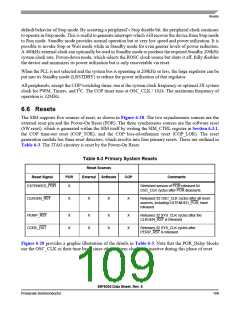
6.5 Power-Saving Modes
The 56F8036 operates in one of five Power-Saving modes, as shown in Table 6-2.
Table 6-2 Clock Operation in Power-Saving Modes
Mode
Core Clocks
Peripheral Clocks
Description
Device is fully functional
Run
Wait
Core and memory
clocks enabled
Peripheral clocks
enabled
Core and memory
clocks disabled
Peripheral clocks
enabled
Core executes WAIT instruction to enter this
mode.
Typically used for power-conscious applications.
Possible recoveries from Wait mode to Run
mode are:
1. Any interrupt
2. Executing a Debug mode entry command
during the 56800E core JTAG interface
3. Any reset (POR, external, software, COP)
Stop
Master clock generation in the OCCS
remains operational, but the SIM disables
the generation of system and peripheral
clocks.
Core executes STOP instruction to enter this
mode.
Possible recoveries from Stop mode to Run
mode are:
1. Interrupt from any peripheral configured in the
CTRL register to operate in Stop mode (TA0-3,
QSCI0, PIT0-1, CAN, CMPA-B)
2. Low-voltage interrupt
3. Executing a Debug mode entry command
using the 56800E core JTAG interface
4. Any reset (POR, external, software, COP)
Standby
The OCCS generates the master clock at a The user configures the OCCS and SIM to select
reduced frequency (400kHz). The PLL is
disabled and the high-speed peripheral
option is not available. System and
peripheral clocks operate at 200kHz.
the relaxation oscillator clock source (PRECS),
shut down the PLL (PLLPD), put the relaxation
oscillator in Standby mode (ROSB), and put the
large regulator in Standby (LRSTDBY). The
device is fully operational, but operating at a
minimum frequency and power configuration.
Recovery requires reversing the sequence used
to enter this mode (allowing for PLL lock time).
Power-Down
Master clock generation in the OCCS is
completely shut down. All system and
peripheral clocks are disabled.
The user configures the OCCS and SIM to enter
Standby mode as shown in the previous
description, followed by powering down the
oscillator (ROPD). The only possible recoveries
from this mode are:
1. External Reset
2. Power-On Reset
The power-saving modes provide additional power management options by disabling the clock,
reconfiguring the voltage regulator clock generation to manage power utilization, as shown in Table 6-2.
Run, Wait, and Stop modes provide methods of enabling/disabling the peripheral and/or core clocking as
a group. Stop disable controls for an individual peripheral are provided in the SDn registers to override the
56F8036 Data Sheet, Rev. 6
108
FreescaleSemiconductor

 FREESCALE [ Freescale ]