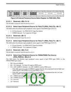
Base + $1A
Read
15
14
13
12
11
10
9
8
7
6
5
4
3
2
1
0
0
0
0
0
0
0
0
0
0
0
0
0
0
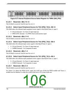
IPS2_
TA3
IPS2_
TA2
IPS2_
TA1
Write
RESET
0
0
0
0
0
0
0
0
0
0
0
0
0
0
0
0
Figure 6-27 Internal Peripheral Source Select Register for TMRA (SIM_IPS2)
6.3.23.1 Reserved—Bits 15–13
This bit field is reserved. Each bit must be set to 0.
6.3.23.2 Select Input Peripheral Source for TA3 (IPS2_TA3)—Bit 12
This field selects the alternate input peripheral source signal to feed Quad Timer A, input 3.
•
•
0 = I/O pin (External) - Use Timer A3 input/output pin
1 = PWM SYNC (Internal) - Use PWM reload synchronization signal
6.3.23.3 Reserved—Bits 11–9
This bit field is reserved. Each bit must be set to 0.
6.3.23.4 Select Input Peripheral Source for TA2 (IPS2_TA2)—Bit 8
This field selects the alternate input source signal to feed Quad Timer A, input 2.
•
•
0 = I/O pin (External) - Use Timer A2 input/output pin
1 = CMPBO (Internal) - Use Comparator B output
6.3.23.5 Reserved—Bits 7–5
This bit field is reserved. Each bit must be set to 0.
6.3.23.6 Select Input Peripheral Source for TA1 (IPS2_TA1)—Bit 4
This field selects the alternate input peripheral source signal to feed Quad Timer A, input 1.
•
•
0 = I/O pin (External) - Use Timer A1 input/output pin
1 = CMPAO (Internal) - Use Comparator A output
6.3.23.7 Reserved—Bits 3–0
This bit field is reserved. Each bit must be set to 0.
For Timer A to detect the PWM SYNC signal, the clock rate of both the PWM module and Timer A
module must be identical, at either the system clock rate or 3X system clock rate.
56F8036 Data Sheet, Rev. 6
106
FreescaleSemiconductor

 FREESCALE [ Freescale ]