Register Descriptions
Base + $18
Read
15
14
13
12
11
10
9
8
7
6
5
4
3
2
1
0
0
0
0
0
0
IPS0_
FAULT2
IPS0_
FAULT1
IPS0_PSRC2
0
IPS0_PSRC1
0
IPS0_PSRC0
0
Write
RESET
0
0
0
0
0
0
0
0
0
0
0
0
0
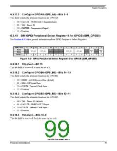
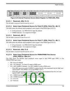
Figure 6-25 Internal Peripheral Source Select Register for PWM (SIM_IPS0)
6.3.21.1 Reserved—Bits 15–14
This bit field is reserved. Each bit must be set to 0.
6.3.21.2 Select Input Peripheral Source for FAULT2 (IPS0_FAULT2)—Bit 13
This field selects the alternate input peripheral source signal to feed PWM input FAULT2.
•
•
0 = I/O Pin (External) - Use PWM FAULT2 Input Pin (default)
1 = CMPBO (Internal) - Use Comparator B Output
6.3.21.3 Reserved—Bit 12
This bit field is reserved. It must be set to 0.
6.3.21.4 Select Input Peripheral Source for FAULT1 (IPS0_FAULT1)—Bit 11
This field selects the alternate input peripheral source signal to feed PWM input FAULT1.
•
•
0 = I/O pin (External) - Use PWM FAULT2 Input Pin (default)
1 = CMPAO (Internal) - Use Comparator A Output
6.3.21.5 Reserved—Bits 10–9
This bit field is reserved. Each bit must be set to 0.
6.3.21.6 Select Input Peripheral Source for PWM4/PWM5 Pair Source
(IPS0_PSRC2)—Bits 8–6
This field selects the alternate input peripheral source signal to feed PWM input PSRC2 as the
PWM4/PWM5 pair source.
•
•
•
000 = Reserved (default)
001 = TA3 (Internal) - Use Timer A3 output as PWM source
010 = ADC SAMPLE2 (Internal) - Use ADC SAMPLE2 result as PWM source
— If the ADC conversion result in SAMPLE2 is greater than the value programmed into the High Limit
register HLMT2, then PWM4 is set to 0 and PWM5 is set to 1
— If the ADC conversion result in SAMPLE2 is less than the value programmed into the Low Limit
register LLMT2, then PWM4 is set to 1 and PWM5 is set to 0
•
•
•
•
011 = CMPAO (Internal) - Use Comparator A output as PWM source
100 = CMPBO (Internal) - Use Comparator B output as PWM source
11x = Reserved
1x1 = Reserved
56F8036 Data Sheet, Rev. 6
Freescale Semiconductor
103

 FREESCALE [ Freescale ]