10.5 External Clock Operation Timing
1
Table 10-10 External Clock Operation Timing Requirements
Characteristic
Symbol
fosc
Min
4
Typ
8
Max
8
Unit
MHz
ns
Frequency of operation (external clock driver)2
Clock Pulse Width3
tPW
6.25
—
—
—
—
—
3
External Clock Input Rise Time4
trise
ns
External Clock Input Fall Time5
tfall
—
3
ns
1. Parameters listed are guaranteed by design.
2. See Figure 10-4 for details on using the recommended connection of an external clock driver.
3. The high or low pulse width must be no smaller than 6.25ns or the chip may not function.
4. External clock input rise time is measured from 10% to 90%.
5. External clock input fall time is measured from 90% to 10%.
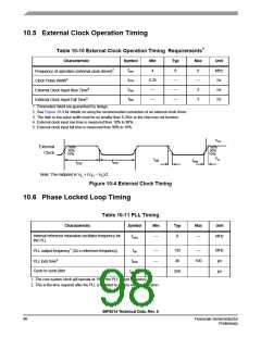
VIH
External
Clock
90%
50%
10%
90%
50%
10%
VIL
tfall
trise
tPW
tPW
Note: The midpoint is VIL + (VIH – VIL)/2.
Figure 10-4 External Clock Timing
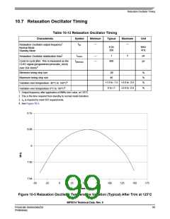
10.6 Phase Locked Loop Timing
Table 10-11 PLL Timing
Characteristic
Symbol
Min
Typ
Max
Unit
Internal reference relaxation oscillator frequency for
the PLL
frosc
—
8
—
MHz
PLL output frequency1 (24 x reference frequency)
fop
tlock
—
—
192
40
—
MHz
µs
PLL lock time2
100
Cycle to cycle jitter
tjitterpll
350
ps
1. The core system clock will operate at 1/6 of the PLL output frequency.
2. This is the time required after the PLL is enabled to ensure reliable operation.
56F8014 Technical Data, Rev. 9
98
Freescale Semiconductor
Preliminary

 FREESCALE [ Freescale ]