General Characteristics
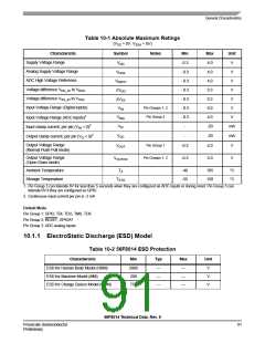
Table 10-1 Absolute Maximum Ratings
(VSS = 0V, VSSA = 0V)
Characteristic
Supply Voltage Range
Symbol
VDD
Notes
Min
-0.3
- 0.3
- 0.3
- 0.3
- 0.3
- 0.3
- 0.3
-
Max
4.0
4.0
4.0
0.3
0.3
6.0
4.0
-20
Unit
V
Analog Supply Voltage Range
ADC High Voltage Reference
VDDA
VREFH
ΔVDD
ΔVSS
VIN
V
V
Voltage difference VDD_IO to VDDA
Voltage difference VSS_IO to VSSA
Input Voltage Range (Digital inputs)
V
V
Pin Groups 1, 2
Pin Group 3
V
Input Voltage Range (ADC inputs)1
Input clamp current, per pin (VIN < 0)2
VINA
V
VIC
mA
Output clamp current, per pin (VO < 0)2
VOC
-
-20
4.0
mA
V
Output Voltage Range
Pin Group 1
VOUT
-0.3
(Normal Push-Pull mode)
Output Voltage Range
(Open Drain mode)
Pin Groups 1, 2
VOUTOD
-0.3
6.0
V
Ambient Temperature
Storage Temperature
TA
-40
-55
105
150
°C
°C
TSTG
1. Pin Group 3 can tolerate 6V for less than 5 seconds when they are configured as ADC inputs or during reset. Pin Group 3 can
tolerate 6V if they are configured as GPIO.
2. Continuous input current per pin is -2 mA
Default Mode
Pin Group 1: GPIO, TDI, TDO, TMS, TCK
Pin Group 2: RESET, GPIOA7
Pin Group 3: ADC analog inputs
10.1.1 ElectroStatic Discharge (ESD) Model
Table 10-2 56F8014 ESD Protection
Characteristic
Min
Typ
Max
Unit
ESD for Human Body Model (HBM)
ESD for Machine Model (MM)
2000
200
—
—
—
—
—
—
V
V
V
ESD for Charge Device Model (CDM)
750
56F8014 Technical Data, Rev. 9
Freescale Semiconductor
Preliminary
91

 FREESCALE [ Freescale ]