Part 9 Joint Test Action Group (JTAG)
9.1 56F8014 Information
Please contact your Freescale sales representative or authorized distributor for device/package-specific
BSDL information.
The TRST pin is not available in this package. The pin is tied to V in the package.
DD
The JTAG state machine is reset during POR and can also be reset via a soft reset by holding TMS high
for five rising edges of TCK, as described in the 56F8000 Peripheral User Manual.
Part 10 Specifications
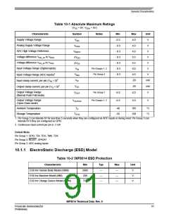
10.1 General Characteristics
The 56F8014 is fabricated in high-density CMOS with 5V-tolerant TTL-compatible digital inputs. The
term “5V-tolerant” refers to the capability of an I/O pin, built on a 3.3V-compatible process technology,
to withstand a voltage up to 5.5V without damaging the device. Many systems have a mixture of devices
designed for 3.3V and 5V power supplies. In such systems, a bus may carry both 3.3V- and 5V-compatible
I/O voltage levels (a standard 3.3V I/O is designed to receive a maximum voltage of 3.3V ± 10% during
normal operation without causing damage). This 5V-tolerant capability therefore offers the power savings
of 3.3V I/O levels, combined with the ability to receive 5V levels without damage.
Absolute maximum ratings in Table 10-1 are stress ratings only, and functional operation at the maximum
is not guaranteed. Stress beyond these ratings may affect device reliability or cause permanent damage to
the device.
Unless otherwise stated, all specifications within this chapter apply over the temperature range of -40ºC to
125ºC ambient temperature over the following supply ranges:
V
= V A = 0V, V = V
= 3.0–3.6V, CL < 50pF, f = 32MHz
SS
SS
DD
DDA
OP
CAUTION
This device contains protective circuitry to guard
against damage due to high static voltage or electrical
fields. However, normal precautions are advised to
avoid application of any voltages higher than
maximum-rated voltages to this high-impedance circuit.
Reliability of operation is enhanced if unused inputs are
tied to an appropriate voltage level.
56F8014 Technical Data, Rev. 9
90
Freescale Semiconductor
Preliminary

 FREESCALE [ Freescale ]