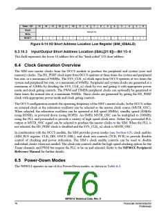
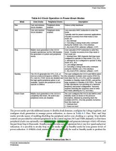
6.7 Clocks
The memory, peripheral and core clocks all operate at the same frequency (32MHz max) with the
exception of the TMR and PWM peripheral clocks, which have the option (using TCR and PCR) to operate
three times faster. The SIM is responsible for stalling individual clocks as a response to various hold-off
requests, low power modes, and other configuration parameters. The SIM has access to the following
signals from the OCCS module:
MSTR_OSC
This comes from the input clock source mux of the OCCS. It is the output of the relaxation oscillator or
the external clock source, depending on PRECS. It is not guaranteed to be at 50% duty cycle (+ or -
10% can probably be assumed for design purposes). This clock runs continuously, even during reset
and is used for reset generation.
HS_PERF
The PLL multiplies the MSTR_OSC by 24, to a maximum of 192MHz. The ZSRC field in OCCS selects
the active source to be the PLL. This is divided by 2 and postscaled to produce this maximum 96MHz
clock. It is used without further division to produce the high-speed (3x system bus rate) variants of the
TMR and PWM peripheral clocks. This clock is disabled when ZSRC is selecting MSTR_OSC.
SYS_CLK_x2
The PLL can multiply the MSTR_OSC by 24, to a maximum of 192MHz. When the PLL is selected by
the OCCS ZSRC field, the PLL is divided by three and postscaled to produce this maximum 64MHz
clock. When MSTR_OSC is selected by the OCCS ZSRC field, MSTR_OSC feeds SYS_CLK_x2
directly. The SIM takes this clock and divides it by two to generate all the normal (1x system bus rate)
peripheral and system clocks.
While the SIM generates the ADC peripheral clock in the same way it generates all other peripheral clocks,
the ADC standby and conversion clocks are generated by a direct interface between the ADC and the
OCCS module.
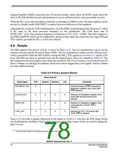
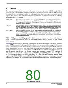
Figure 6-16 illustrates clock relationships to one another and to the various resets as the device comes out
of reset. RST is assumed to be the logical AND of all active-low system resets (for example, POR, external
reset, COP and Software reset). In the 56F8014 architecture, this signal will be stretched by the SIM for a
period of time (up to 96 MSTR_OSC clock cycles, depending upon the status of the POR) to create the
clock generation reset signal (CLKGEN_RST). The SIM should deassert CLKGEN_RST synchronously
with the negative edge of OSC_CLK in order to avoid skew problems. CLKGEN_RST is delayed 32
SYS_CLK cycles to create the peripheral reset signal (PERIP_RST). PERIP_RST is then delayed by 32
SYS_CLK cycles to create CORE_RST. Both PERIP_RST and CORE_RST should be released on the
negative edge of SYS_CLK_D as shown. This phased releasing of system resets is necessary to give some
peripherals (for example, the Flash interface unit) set-up time prior to the 56800E core becoming active.
56F8014 Technical Data, Rev. 9
80
Freescale Semiconductor
Preliminary

 FREESCALE [ Freescale ]