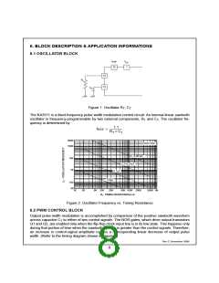
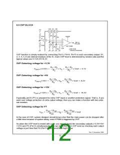
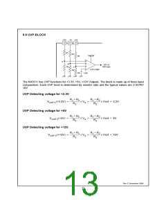
6.5 OVP BLOCK
3.3V 5V 12V
VO
13
14 15
R1
R2
R101
PT
R3
Vref=5V
R5
16
D
A
SET of
R/S Latch
B
C
R102
OVP COMP
R4
1.25V
R6
R102, R102
: External Components
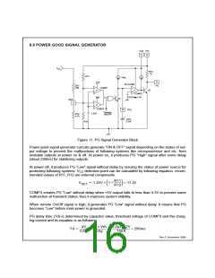
OVP function is simply realized by connecting Pin13, Pin14, Pin15 to each secondary output. R1,
2, 3, 4, 5, 6 are internal resistors of the IC. Each OVP level is determined by resistor ratio and the
typical values are 4.1V/6.2V/14.2V.
OVP Detecting voltage for +3.3V
+
+
R1 R2
R1 R2
(
) = -------------------- ×
= -------------------- ×
=
VOVP 1 +3.3V
VA
Vref
Vref
Vref
4.1V
6.2V
R2
R2
OVP Detecting voltage for +5V
+
+
R3 R4
R3 R4
--------------------
--------------------
(
) =
×
=
VB
×
=
VOVP 2 +5V
R4
R4
OVP Detecting voltage for +12V
+
+
R5 R6
R5 R6
(
) = -------------------- ×
= -------------------- ×
=
14.2V
VOVP 3 +12V
VC
R6
R6
Especially, pin16 (PT) is prepared for extra OVP input or another protection signal. That is, if you
want over voltage protection of extra output voltage, then you can make a function with two exter-
nal resistors.
OVP Detecting voltage for PT
+
+
R101 R102
R101 R102
= ------------------------------ ×
= ------------------------------ ×
VPT
VD
Vref
R102
R102
In the case of OVP, system designer should know a fact that the main power can be dropped after
a little time because of system delay, even if PWM is triggered by OVP.
So when the OVP level is tested with a set, you should check the secondary outputs (+3.3V/+5V/
+12V) and PG (Pin11) simultaneously. you can know the each OVP level as checking each output
voltage in just time that PG (Pin11) is triggered from high to low.
Rev C, November 1999
12

 FAIRCHILD [ FAIRCHILD SEMICONDUCTOR ]