Recommended Operating Conditions
Value
Symbol
Parameter
Conditions
Units
Min. Typ. Max.
VPN
VCC
VBS
Supply Voltage
Applied between P - NU, NV, NW
-
300
15
15
-
400
16.5
18.5
1
V
V
Control Supply Voltage
High-side Bias Voltage
Applied between VCC(H), VCC(L)-COM
Applied between VB(U)-VS(U), VB(V)-VS(V),VB(W)-VS(W)
13.5
13.0
-1
V
dVCC/dt, Control supply variation
dVBS/dt
V/ms
tdead
Blanking Time for
Preventing Arm-short
For Each Input Signal
1.5
-
-
-
ms
fPWM
VSEN
PWM Input Signal
-40°C < TJ < 150°C
-
20
4
kHz
V
Voltage for Current
Sensing
Applied between NU, NV, NW - COM
(Including surge voltage)
-4
PWIN(ON) Minimun Input Pulse
(Note 7)
0.5
0.5
-
-
-
-
ms
Width
PWIN(OFF)
Note:
7. SPM might not make response if input pulse width is less than the recommanded value.
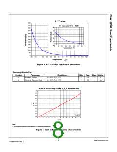
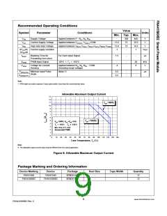
Allowable Maximum Output Current
13
12
11
10
9
fSW=5kHz
8
7
6
5
fSW=15kHz
VDC=300V, VCC=VBS=15V
4
TJ < 150℃ , TC ≤ 125℃
3
M.I.=0.9, P.F.=0.8
Sinusoidal PWM
2
1
0
0
10
20
30
40
50
60
70
80
90 100 110 120 130 140
Case Temperature, TC [℃]
Note:
8. The allowable output current value may be different from the actual application.
Figure 8. Allowable Maximum Output Current
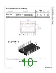
Package Marking and Ordering Information
Device Marking
FNA41560
Device
FNA41560
FNA41560B2
Package
SPM26-AAA
SPM26-AAC
Reel Size
Tape Width
Quantity
-
-
-
-
12
12
FNA41560B2
9
www.fairchildsemi.com
FNA41560/B2 Rev. C

 FAIRCHILD [ FAIRCHILD SEMICONDUCTOR ]