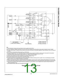
HVIC
(26) VB(U)
P (3)
U (4)
VB(U)
CBS
CBS
CBS
CBSC
(25) VS(U)
(20) IN
VS(U)
OUT(UH)
VS(U)
RS
(UH)
IN(UH)
VB(V)
Gating UH
Gating VH
Gating WH
(24) VB(V)
(23) VS(V)
CBSC
VS(V)
RS
(19) IN
(VH)
OUT(VH)
VS(V)
IN(VH)
V (5)
(22) VB(W)
(21) VS(W)
M
VB(W)
VS(W)
CBSC
RS
(18) IN
(WH)
CDCS
VDC
IN(WH)
VCC
M
C
U
OUT(WH)
VS(W)
(17) VCC(H)
(15) COM
15V line
W (6)
CPS CPS
CPS
CSPC15
CSP15
COM
5V line
LVIC
(16) VCC(L)
VCC
VFO
OUT(UL)
OUT(VL)
OUT(WL)
RPF
RSU
NU (7)
NV (8)
NW (9)
CSPC05
CSP05
RS
(11) VFO
Fault
CPF
CBPF
RS
(14) IN
(UL)
RSV
Gating UL
Gating VL
Gating WL
IN(UL)
IN(VL)
RS
RS
(13) IN
(VL)
(12) IN
(WL)
IN(WL)
COM
CSC
CSC
(10) CSC
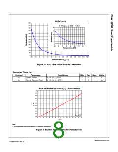
(1) VTH
(2) RTH
CPS CPS
CPS
RSW
RF
THERMISTOR
RTH
U-Phase Current
V-Phase Current
W-Phase Current
Input Signal for
Short-Circuit Protection
Temp. Monitoring
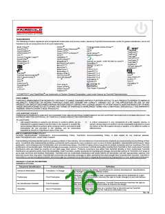
Note:
1) To avoid malfunction, the wiring of each input should be as short as possible. (less than 2-3cm)
2) By virtue of integrating an application specific type HVIC inside the SPM, direct coupling to CPU terminals without any opto-coupler or transformer isolation is possible.
3) V output is open drain type. This signal line should be pulled up to the positive side of the MCU or control power supply with a resistor that makes I up to 1mA. Please refer
FO
FO
to Figure14.
4) C
of around 7 times larger than bootstrap capacitor C is recommended.
BS
SP15
5) Input signal is High-Active type. There is a 5kW resistor inside the IC to pull down each input signal line to GND. RC coupling circuits is recommanded for the prevention
of input signal oscillation. R time constant should be selected in the range 50~150ns. (Recommended R =100Ω, C =1nF)
C
S
PS
S
PS
6) To prevent errors of the protection function, the wiring around R and C should be as short as possible.
F
SC
7) In the short-circuit protection circuit, please select the R C time constant in the range 1.5~2ms.
F
SC
8) Each capacitor should be mounted as close to the pins of the SPM as possible.
9) To prevent surge destruction, the wiring between the smoothing capacitor and the P&GND pins should be as short as possible. The use of a high frequency non-inductive
capacitor of around 0.1~0.22mF between the P&GND pins is recommended.
10) Relays are used at almost every systems of electrical equipments of home appliances. In these cases, there should be sufficient distance between the CPU and the relays.
11) The zener diode should be adopted for the protection of ICs from the surge destruction between each pair of control supply terminals. (Recommanded zener diode=24V/1W)
12) Please choose the electrolytic capacitor with good temperature characteristic in C . Also, choose 0.1~0.2mF R-category ceramic capacitors with good temperature and
BS
frequency characteristics in C
.
BSC
13) For the detailed information, please refer to the AN-9070 and FEB305-001.
Figure 15. Typical Application Circuit
13
www.fairchildsemi.com
FNA41560/B2 Rev. C

 FAIRCHILD [ FAIRCHILD SEMICONDUCTOR ]