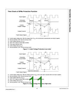
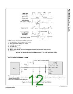
Lower arms
control input
c6
c7
Protection
Circuit state
SET
RESET
Internal IGBT
Gate-Emitter Voltage
c4
c3
c2
SC
c1
c8
Output Current
SC Reference Voltage
Sensing Voltage
of the shunt
resistance
CR circuit time
constant delay
c5
Fault Output Signal
(with the external shunt resistance and CR connection)
c1 : Normal operation: IGBT ON and carrying current.
c2 : Short circuit current detection (SC trigger).
c3 : Hard IGBT gate interrupt.
c4 : IGBT turns OFF.
c5 : Input “L” : IGBT OFF state.
c6 : Input “H”: IGBT ON state, but during the active period of fault output the IGBT doesn’t turn ON.
c7 : IGBT OFF state
Figure 13. Short-Circuit Current Protection (Low-side Operation only)
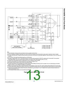
Input/Output Interface Circuit
5V-Line (MCU or Control power)
RPF=10kΩ
SPM
,
,
IN(UH) IN(VH)
IN(WH)
,
,
IN(UL) IN(VL)
IN(WL)
MCU
VFO
COM
Note:
1) RC coupling at each input (parts shown dotted) might change depending on the PWM control scheme used in the application and the wiring impedance of the application’s
printed circuit board. The SPM input signal section integrates 5kW (typ.) pull-down resistor. Therefore, when using an external filtering resistor, please pay attention to the sig-
nal voltage drop at input terminal.
2) The logic input is compatible with standard CMOS outputs.
Figure 14. Recommended CPU I/O Interface Circuit
12
www.fairchildsemi.com
FNA41560/B2 Rev. C

 FAIRCHILD [ FAIRCHILD SEMICONDUCTOR ]