Electrical Characteristics (TJ = 25°C, Unless Otherwise Specified)
Inverter Part
Symbol
Parameter
Conditions
Min. Typ. Max. Units
VCE(SAT)
Collector-Emitter Saturation VCC = VBS = 15V
IC = 15A, TJ = 25°C
-
1.8
2.3
V
Voltage
VIN = 5V
VF
FWD Forward Voltage
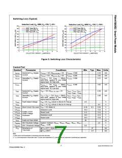
Switching Times
VIN = 0V
IF = 15A, TJ = 25°C
-
1.8
0.75
0.25
0.75
0.25
0.15
0.75
0.25
0.75
0.25
0.15
-
2.3
1.25
0.50
1.25
0.50
-
V
ms
ms
ms
ms
ms
ms
ms
ms
ms
ms
mA
HS
tON
tC(ON)
tOFF
tC(OFF)
trr
VPN = 300V, VCC = VBS = 15V, IC = 15A
TJ = 25°C
VIN = 0V « 5V, Inductive Load
(Note 3)
0.45
-
-
-
-
LS
tON
VPN = 300V, VCC = VBS = 15V, IC = 15A
TJ = 25°C
VIN = 0V « 5V, Inductive Load
(Note 3)
0.45
1.25
0.50
1.25
0.50
-
tC(ON)
tOFF
tC(OFF)
trr
-
-
-
-
-
ICES
Collector-Emitter
Leakage Current
VCE = VCES
1
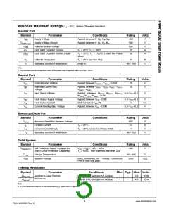
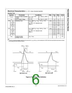
Note:
3.
t
and t
include the propagation delay time of the internal drive IC. t
and t
are the switching time of IGBT itself under the given gate driving condition internally.
C(OFF)
ON
OFF
C(ON)
For the detailed information, please see Figure 4.
100% IC 100% IC
trr
VCE
IC
IC
VCE
VIN
VIN
tON
tOFF
tC(ON)
tC(OFF)
10% IC
VIN(ON)
VIN(OFF)
10% VCE
10% IC
10% VCE
90% IC
(b) turn-off
(a) turn-on
Figure 4. Switching Time Definition
6
www.fairchildsemi.com
FNA41560/B2 Rev. C

 FAIRCHILD [ FAIRCHILD SEMICONDUCTOR ]