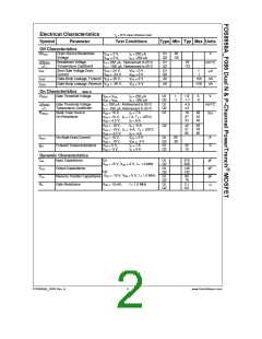
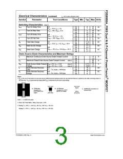
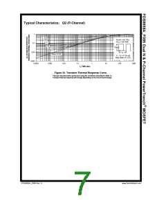
Typical Characteristics: Q1 (N-Channel)
20
2.2
1.8
1.4
1
VGS = 10.0V
4.0V
3.5V
16
12
8
VGS = 3.5V
6.0V
4.5V
4.0
4.5V
5.0
6.0V
3.0V
10.0V
16
4
0
0.6
0
0.5
1
1.5
2
0
4
8
12
20
VDS, DRAIN-SOURCE VOLTAGE (V)
ID, DRAIN CURRENT (A)
Figure 1. On-Region Characteristics.
Figure 2. On-Resistance Variation with
Drain Current and Gate Voltage.
1.6
1.4
1.2
1
0.08
0.07
0.06
0.05
0.04
0.03
0.02
0.01
ID = 7A
VGS = 10.0V
ID = 3.5A
TA = 125oC
TA = 25oC
0.8
0.6
-50
-25
0
25
50
75
100
125
150
2
4
6
8
10
TJ, JUNCTION TEMPERATURE (oC)
VGS, GATE TO SOURCE VOLTAGE (V)
Figure 3. On-Resistance Variation with
Temperature.
Figure 4. On-Resistance Variation with
Gate-to-Source Voltage.
20
16
12
8
100
VGS = 0V
VDS = 5V
10
TA = 125oC
1
0.1
TA = 125oC
-55oC
25oC
25oC
0.01
-55oC
4
0.001
0.0001
0
1.5
2
2.5
3
3.5
4
0
0.2
0.4
0.6
0.8
1
1.2
VGS, GATE TO SOURCE VOLTAGE (V)
VSD, BODY DIODE FORWARD VOLTAGE (V)
Figure 5. Transfer Characteristics.
Figure 6. Body Diode Forward Voltage Variation
with Source Current and Temperature.
FDS8958A_F085 Rev. A
4
www.fairchildsemi.com

 FAIRCHILD [ FAIRCHILD SEMICONDUCTOR ]