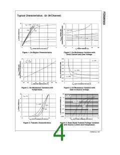
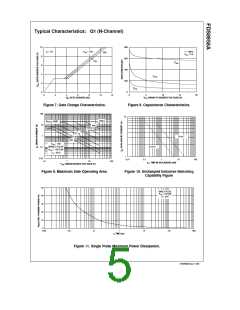
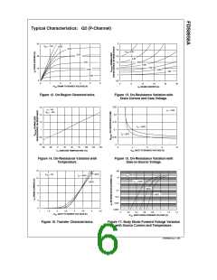
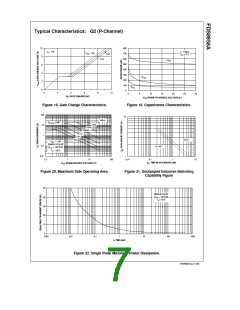
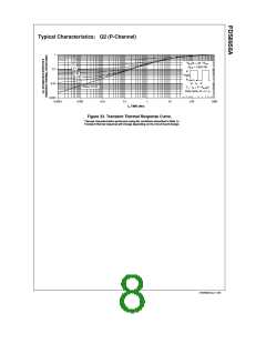
Typical Characteristics: Q1 (N-Channel)
20
2.2
1.8
1.4
1
VGS = 10.0V
4.0V
3.5V
16
12
8
VGS = 3.5V
6.0V
4.5V
4.0
4.5V
5.0
6.0V
3.0V
10.0V
16
4
0
0.6
0
0.5
1
1.5
2
0
4
8
12
20
VDS, DRAIN-SOURCE VOLTAGE (V)
ID, DRAIN CURRENT (A)
Figure 1. On-Region Characteristics.
Figure 2. On-Resistance Variation with
Drain Current and Gate Voltage.
1.6
1.4
1.2
1
0.08
0.07
0.06
0.05
0.04
0.03
0.02
0.01
ID = 7A
VGS = 10.0V
ID = 3.5A
TA = 125oC
TA = 25oC
0.8
0.6
-50
-25
0
25
50
75
100
125
150
2
4
6
8
10
TJ, JUNCTION TEMPERATURE (oC)
VGS, GATE TO SOURCE VOLTAGE (V)
Figure 3. On-Resistance Variation with
Temperature.
Figure 4. On-Resistance Variation with
Gate-to-Source Voltage.
20
16
12
8
100
VGS = 0V
VDS = 5V
10
TA = 125oC
1
0.1
TA = 125oC
-55oC
25oC
25oC
0.01
-55oC
4
0.001
0.0001
0
1.5
2
2.5
3
3.5
4
0
0.2
0.4
0.6
0.8
1
1.2
VGS, GATE TO SOURCE VOLTAGE (V)
VSD, BODY DIODE FORWARD VOLTAGE (V)
Figure 5. Transfer Characteristics.
Figure 6. Body Diode Forward Voltage Variation
with Source Current and Temperature.
FDS8958A Rev F1 (W)

 FAIRCHILD [ FAIRCHILD SEMICONDUCTOR ]