February 2007
tm
FDS8958A
Dual N & P-Channel PowerTrench MOSFET
General Description
Features
These dual N- and P-Channel enhancement mode
power field effect transistors are produced using
Fairchild Semiconductor’s advanced PowerTrench
process that has been especially tailored to minimize
on-state ressitance and yet maintain superior switching
performance.
•
Q1:
N-Channel
7.0A, 30V
RDS(on) = 0.028Ω @ VGS = 10V
RDS(on) = 0.040Ω @ VGS = 4.5V
•
Q2:
P-Channel
-5A, -30V
RDS(on) = 0.052Ω @ VGS = -10V
RDS(on) = 0.080Ω @ VGS = -4.5V
These devices are well suited for low voltage and
battery powered applications where low in-line power
loss and fast switching are required.
•
•
Fast switching speed
High power and handling capability in a widely
used surface mount package
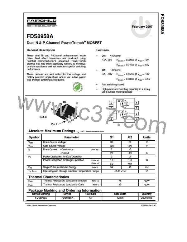
Q2
D2
D
5
6
7
8
4
3
2
1
D2
D
D1
D
D1
D
Q1
G2
SO-8
S2
G
G1
S
S1
S
SO-8
Pin 1
S
Absolute Maximum Ratings TA = 25°C unless otherwise noted
Symbol
Parameter
Q1
Q2
Units
VDSS
VGSS
ID
Drain-Source Voltage
30
±20
7
30
±20
-5
V
V
Gate-Source Voltage
Drain Current - Continuous
- Pulsed
(Note 1a)
A
20
2
-20
2
PD
Power Dissipation for Dual Operation
Power Dissipation for Single Operation
W
(Note 1a)
(Note 1c)
1.6
0.9
54
1.6
0.9
13
EAS
Single Pulse Avalanche Energy
(Note 3)
mJ
TJ, TSTG
Operating and Storage Junction Temperature Range
-55 to +150
°C
Thermal Characteristics
Thermal Resistance, Junction-to-Ambient
Thermal Resistance, Junction-to-Case
(Note 1a)
(Note 1)
78
40
RθJA
RθJC
°C/W
°C/W
Package Marking and Ordering Information
Device Marking
Device
Reel Size
Tape width
Quantity
FDS8958A
FDS8958A
13”
12mm
2500 units
FDS8958A Rev F1(W)
2007 Fairchild Semiconductor Corporation

 FAIRCHILD [ FAIRCHILD SEMICONDUCTOR ]