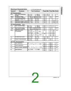
Electrical Characteristics (continued)
TA = 25°C unless otherwise noted
Symbol Parameter Test Conditions
Type Min Typ Max Units
Switching Characteristics (Note 2)
td(on)
tr
td(off)
tf
Turn-On Delay Time
Turn-On Rise Time
Turn-Off Delay Time
Turn-Off Fall Time
Total Gate Charge
Gate-Source Charge
Gate-Drain Charge
Q1
Q1
Q2
Q1
Q2
Q1
Q2
Q1
Q2
Q1
Q2
Q1
Q2
Q1
Q2
8
7
5
13
23
14
3
16
14
10
24
37
25
6
17
26
13
ns
ns
V
DD = 15 V, ID = 1 A,
VGS = 10V, RGEN = 6 Ω
Q2
ns
VDD = -15 V, ID = -1 A,
VGS = -10V, RGEN = 6 Ω
ns
9
Qg
Qgs
Qgd
Q1
10.7
9.6
1.7
2.2
2.1
1.7
nC
nC
nC
VDS = 15 V, ID = 7 A, VGS = 10 V
Q2
VDS = -15 V, ID = -5 A,VGS = -10 V
Drain–Source Diode Characteristics and Maximum Ratings
IS
Maximum Continuous Drain-Source Diode Forward Current
Q1
Q2
Q1
Q2
Q1
Q2
Q1
Q2
1.3
-1.3
1.2
A
V
VSD
trr
Drain-Source Diode Forward VGS = 0 V, IS = 1.3 A
(Note 2)
(Note 2)
0.75
-0.88
19
19
9
Voltage
VGS = 0 V, IS = -1.3 A
-1.2
Diode Reverse Recovery
Time
Diode Reverse Recovery
Charge
Q1
nS
nC
IF = 7 A, diF/dt = 100 A/µs
Q2
Qrr
IF = -5 A, diF/dt = 100 A/µs
6
Notes:
1. RθJA is the sum of the junction-to-case and case-to-ambient thermal resistance where the case thermal reference is defined as the solder mounting surface of
the drain pins. RθJC is guaranteed by design while RθCA is determined by the user's board design.
a) 78°/W when
mounted on a
0.5 in2 pad of 2 oz
copper
b) 125°/W when
c) 135°/W when mounted on a
minimum pad.
mounted on a .02 in2
pad of 2 oz copper
Scale 1 : 1 on letter size paper
2. Pulse Test: Pulse Width < 300µs, Duty Cycle < 2.0%
3. Starting TJ = 25°C, L = 3mH, IAS = 6A, VDD = 30V, VGS = 10V (Q1).
Starting TJ = 25°C, L = 3mH, IAS = 3A, VDD = 30V, VGS = 10V (Q2).
FDS8958A Rev F1 (W)

 FAIRCHILD [ FAIRCHILD SEMICONDUCTOR ]