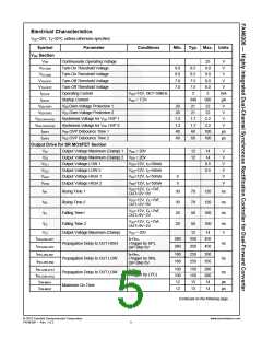
Electrical Characteristics
VDD=20V, TA=25Ԩ, unless otherwise specified.
Symbol
Parameter
Conditions
Min.
Typ. Max. Units
VDD Section
VOP
Continuously Operating Voltage
Turn-On Threshold Voltage
Turn-On Threshold Voltage
Turn-Off Threshold Voltage
Turn-Off Threshold Voltage
Operating Current
25
9.0
9.0
8.0
8.0
5
V
V
VTH-ON1
VTH-ON2
VTH-OFF1
VTH-OFF2
IDD-OP
8.0
8.0
7.0
7.0
8.5
8.5
7.5
7.5
3
V
V
V
VDD=15V, DET=50KHz
VDD = 7.5V
mA
μA
V
IDD-ST
Startup Current
340
21
500
22
VDD-OVP1
VDD-OVP2
VDD-OVP-HYS1
VDD-OVP-HYS2
tOVP1
VDD Over-Voltage Protection 1
VDD Over-Voltage Protection 2
Hysteresis Voltage for VDD OVP 1
Hysteresis Voltage for VDD OVP 2
VDD OVP Debounce Time 1
VDD OVP Debounce Time 2
20
20
21
22
V
1.2
1.2
40
1.7
1.7
60
2.2
2.2
100
100
V
V
μs
μs
tOVP2
40
60
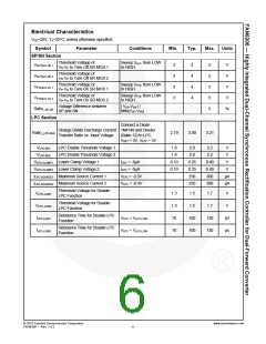
Output Drive for SR MOSFET Section
VZ1
VZ2
Output Voltage Maximum (Clamp) 1 VDD = 20V
Output Voltage Maximum (Clamp) 2 VDD = 20V
12
12
14
14
V
V
V
V
V
V
VOL1
VOL2
VOH1
VOH2
Output Voltage LOW 1
Output Voltage LOW 2
Output Voltage HIGH 1
Output Voltage HIGH 2
VDD=12V, IO=50mA
VDD=12V, IO=50mA
VDD=12V, IO=50mA
VDD=12V, IO=50mA
0.5
0.5
9
9
VDD=12V, CL=7nF,
OUT=2V~9V
tR1
tR2
tF1
tF2
Rising Time 1
Rising Time 2
Falling Time1
30
30
20
20
70
70
50
50
120
120
100
100
ns
ns
ns
VDD=12V, CL=7nF,
OUT=2V~9V
VDD=12V, CL=7nF,
OUT=9V~2V
VDD=12V, CL=7nF,
OUT=9V~2V
Falling Time 2
ns
V
VZ1
Output Voltage Maximum (Clamp)
VDD = 20V
12
14
tPD-HIGH-SP1
tR+tPD
(Trigger by SP),
|SP-SN|=5V
,
280
280
180
180
350
450
Propagation Delay to OUT HIGH
Propagation Delay to OUT LOW
ns
tPD-HIGH-SP2
tPD-LOW-SN1
tPD-LOW-SN2
350
250
250
450
350
350
tR+tPD
,
(Trigger by SN),
|SP-SN|=5V
ns
ns
tPD-LOW-LPC1
tPD-LOW-LPC2
tON-MAX1
100
100
12
150
150
13
200
200
14
tR+tPD
(Trigger by LPC)
,
Propagation Delay to OUT LOW
Maximum On Time
μs
μs
tON-MAX2
12
13
14
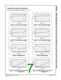
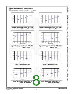
Continued on the following page…
© 2010 Fairchild Semiconductor Corporation
FAN6206 • Rev. 1.0.2
www.fairchildsemi.com
5

 FAIRCHILD [ FAIRCHILD SEMICONDUCTOR ]