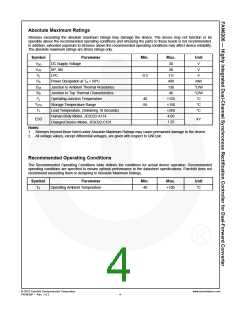
Absolute Maximum Ratings
Stresses exceeding the absolute maximum ratings may damage the device. The device may not function or be
operable above the recommended operating conditions and stressing the parts to these levels is not recommended.
In addition, extended exposure to stresses above the recommended operating conditions may affect device reliability.
The absolute maximum ratings are stress ratings only.
Symbol
Parameter
Min.
Max.
Unit
VDD
VHV
VL
DC Supply Voltage
SP, SN
30
30
V
V
LPC
-0.3
7.0
V
PD
Power Dissipation at TA < 50°C
400
130
46
mW
°C/W
°C/W
°C
ΘJA
Ψjt
Junction to Ambient Thermal Resistance
Junction to Top Thermal Characteristics
Operating Junction Temperature
TJ
-40
-55
+125
+150
+260
4.00
1.25
TSTG
TL
Storage Temperature Range
°C
Lead Temperature, (Soldering 10 Seconds)
Human Body Model, JESD22-A114
Charged Device Model, JESD22-C101
°C
ESD
kV
Notes:
1. Stresses beyond those listed under Absolute Maximum Ratings may cause permanent damage to the device.
2. All voltage values, except differential voltages, are given with respect to GND pin.
Recommended Operating Conditions
The Recommended Operating Conditions table defines the conditions for actual device operation. Recommended
operating conditions are specified to ensure optimal performance to the datasheet specifications. Fairchild does not
recommend exceeding them or designing to Absolute Maximum Ratings.
Symbol
Parameter
Min.
Max.
Unit
TA
Operating Ambient Temperature
-40
+105
°C
© 2010 Fairchild Semiconductor Corporation
FAN6206 • Rev. 1.0.2
www.fairchildsemi.com
4

 FAIRCHILD [ FAIRCHILD SEMICONDUCTOR ]