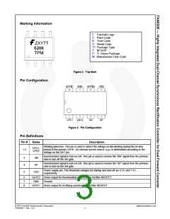
Marking Information
F: Fairchild Logo
Z: Plant Code
X: Year Code
Y: Week Code
TT: Package Type
T: M=SOP
P: Y: Green Package
M: Manufacture Flow Code
Figure 3. Top Mark
Pin Configuration
Figure 4. Pin Configuration
Description
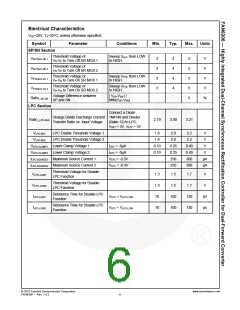
Pin Definitions
Pin #
Name
Winding detection. This pin is used to detect the voltage on the winding during the on-time
period of the primary GATE. An internal current source, ICHG, is determined according to the
voltage on the DET pin.
LPC1,
LPC2
1,2
Synchronized signal to turn on SR. This pin is used to receive the “XN” signal from the primary
side to turn off the SR gate.
3
4
5
SN
SP
Synchronized signal to turn on SR. This pin is used to receive the “XP” signal from the primary-
side to turn-on the SR gate.
Power supply pin. The threshold voltages for startup and turn-off are 8.5V and 7.5V,
respectively.
VDD
6
7
8
GATE2 Driver output for freewheeling synchronous rectifier MOSFET.
GND Ground
GATE1 Driver output for rectifying synchronous rectifier MOSFET.
© 2010 Fairchild Semiconductor Corporation
FAN6206 • Rev. 1.0.2
www.fairchildsemi.com
3

 FAIRCHILD [ FAIRCHILD SEMICONDUCTOR ]