FSDH321, FSDL321
Functional Description
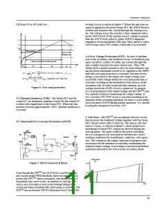
1. Startup : In previous generations of Fairchild Power
Switches (FPSTM) the Vstr pin had an external resistor to the
DC input voltage line. In this generation the startup resistor
is replaced by an internal high voltage current source and a
switch that shuts off when 15mS goes by after the supply
voltage, Vcc, gets above 12V. The source turns back on if
Vcc drops below 8V.
Vcc
5uA
Vref
0.9mA
FB
3
Vfb
Vo
OSC
D1
D2
Cfb
2.5R
R
Vfb*
Gate
driver
431
OLP
VSD
Vin,dc
Istr
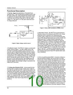
Figure 5. Pulse width modulation (PWM) circuit
Vstr
Vcc
UVLO <8V
on
4. Protection Circuit : The FPSTM has several protective
functions such as over load protection (OLP), over voltage
protection (OVP), abnormal over current protection
(AOCP), under voltage lock out (UVLO) and thermal shut-
down (TSD). Because these protection circuits are fully inte-
grated inside the IC without external components, the
reliability is improved without increasing cost. Once the
fault condition occurs, switching is terminated and the Sense
FET remains off. This causes Vcc to fall. When Vcc reaches
the UVLO stop voltage, 8V, the protection is reset and the
internal high voltage current source charges the Vcc capaci-
tor via the Vstr pin. When Vcc reaches the UVLO start volt-
age,12V, the FPSTM resumes its normal operation. In this
manner, the auto-restart can alternately enable and disable
the switching of the power Sense FET until the fault condi-
tion is eliminated.
J-FET
15mS After UVLO
start(>12V)
off
Figure 4. High voltage current source
2. Feedback Control : The FSDx321 employs current mode
control, shown in figure 5. An opto-coupler (such as the
H11A817A) and shunt regulator (such as the KA431) are
typically used to implement the feedback network. Compar-
ing the feedback voltage with the voltage across the Rsense
resistor plus an offset voltage makes it possible to control the
switching duty cycle. When the reference pin voltage of the
KA431 exceeds the internal reference voltage of 2.5V, the
H11A817A LED current increases, thus pulling down the
feedback voltage and reducing the duty cycle. This event
typically happens when the input voltage is increased or the
output load is decreased.
4.1 Over Load Protection (OLP) : Overload is defined as
the load current exceeding a pre-set level due to an unex-
pected event. In this situation, the protection circuit should
be activated in order to protect the SMPS. However, even
when the SMPS is in the normal operation, the over load
protection circuit can be activated during the load transition.
In order to avoid this undesired operation, the over load pro-
tection circuit is designed to be activated after a specified
time to determine whether it is a transient situation or an
overload situation. In conjunction with the Ipk current limit
pin (if used) the current mode feedback path would limit the
current in the Sense FET when the maximum PWM duty
cycle is attained. If the output consumes more than this max-
imum power, the output voltage (Vo) decreases below the set
voltage. This reduces the current through the opto-coupler
LED, which also reduces the opto-coupler transistor current,
thus increasing the feedback voltage (Vfb). If Vfb exceeds
3V, the feedback input diode is blocked and the 5uA Idelay
current source starts to charge Cfb slowly up to Vcc. In this
condition, Vfb continues increasing until it reaches 6V, when
the switching operation is terminated as shown in figure 6.
The delay time for shutdown is the time required to charge
3. Leading edge blanking (LEB) : At the instant the inter-
nal Sense FET is turned on, there usually exists a high cur-
rent spike through the Sense FET, caused by the primary side
capacitance and secondary side rectifier diode reverse recov-
ery. Excessive voltage across the Rsense resistor would lead
to incorrect feedback operation in the current mode PWM
control. To counter this effect, the FPSTM employs a leading
edge blanking (LEB) circuit. This circuit inhibits the PWM
comparator for a short time (T
turned on.
) after the Sense FET is
LEB
10

 FAIRCHILD [ FAIRCHILD SEMICONDUCTOR ]