XRT86L30
REV. 1.0.1
SINGLE T1/E1/J1 FRAMER/LIU COMBO
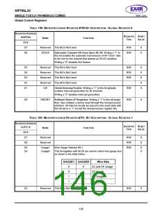
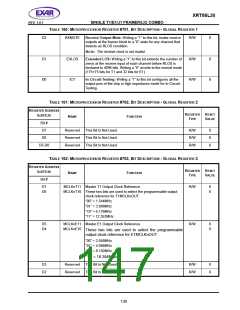
TABLE 160: MICROPROCESSOR REGISTER #701, BIT DESCRIPTION - GLOBAL REGISTER 1
D2
RXMUTE
Receive Output Mute: Writing a “1” to this bit, mutes receive
outputs at the framer block to a “0” state for any channel that
detects an RLOS condition.
R/W
0
NOTE: The receive clock is not muted.
D1
D0
EXLOS
ICT
Extended LOS: Writing a “1” to this bit extends the number of
zeros at the receive input of each channel before RLOS is
declared to 4096 bits. Writing a “0” reverts to the normal mode
(175+75 bits for T1 and 32 bits for E1).
R/W
R/W
0
0
In-Circuit-Testing: Writing a “1” to this bit configures all the
output pins of the chip in high impedance mode for In-Circuit-
Testing.
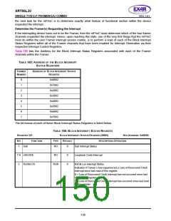
TABLE 161: MICROPROCESSOR
R
EGISTER #702, BIT DESCRIPTION - GLOBAL REGISTER 2
R
EGISTER ADDRESS
R
EGISTER
YPE
R
VALUE
ESET
0x0FE2h
N
AME
FUNCTION
T
Bit #
D7
Reserved
Reserved
Reserved
This Bit Is Not Used
This Bit Is Not Used
This Bit Is Not Used
R/W
R/W
R/W
0
0
0
D6
D5-D0
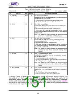
TABLE 162: MICROPROCESSOR
R
EGISTER #703, BIT
D
ESCRIPTION - GLOBAL
R
EGISTER
3
R
EGISTER
A
DDRESS
R
EGISTER
YPE
R
VALUE
ESET
0x0FE4h
N
AME
FUNCTION
T
Bit #
D7
D6
MCLKnT11 Master T1 Output Clock Reference
R/W
0
0
MCLKnT10 These two bits are used to select the programmable output
clock reference for T1MCLKnOUT.
“00” = 1.544MHz
“01” = 3.088MHz
“10” = 6.176MHz
“11” = 12.352MHz
D5
D4
MCLKnE11 Master E1 Output Clock Reference
MCLKnE10
R/W
0
0
These two bits are used to select the programmable
output clock reference for E1MCLKnOUT.
“00” = 2.048MHz
“01” = 4.096MHz
“10” = 8.192MHz
“11” = 16.384MHz
This Bit Is Not Used.
This Bit Is Not Used.
D3
D2
Reserved
Reserved
R/W
R/W
0
0
136

 EXAR [ EXAR CORPORATION ]