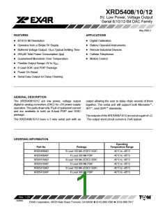
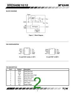
XRD5408/10/12
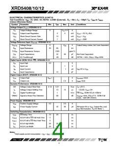
ELECTRICAL CHARACTERISTICS (CONT’D)
Test Conditions: V = 5V, GND= 0V, REFIN= 2.048V (External), R = 10kΩ, C = 100pF, T = T
to T
,
MAX
DD
L
L
A
MIN
Unless Otherwise Noted.
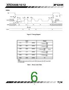
Symbol
tDS
Parameter
Min.
10
0
Typ.
Max.
Unit
ns
Conditions
DIN Setup Time
45
tDH
DIN Hold Time
ns
tDO
DOUT Valid Propagation Delay
CS High Pulse Width
8
15
ns
CL= 50pF
tCSW
tCS1
20
10
40
20
ns
CS Rise to SCLK Rise Setup
Time
ns
Specifications are subject to change without notice
ABSOLUTE MAXIMUM RATINGS
V
DD
to GND . . . . . . . . . . . . . . . . . . . . . . . . . . -0.3V, +7V
Package Power Dissipation Ratings (T = +70°C)
A
PDIP (derate 9mW/°C above +70°C) . . . . 117mW
SOIC (derate 6mW/°C above +70°C) . . . 155mW
Operating Temperature Range . . . . . -40°C to + 85°C
Storage Temperature Range . . . . . . -65°C to +165°C
Lead Temperature (soldering, 10 sec) . . . . . . +300°C
Digital Input Voltage to GND . . . . . . -0.3V, V +0.3V
DD
V
V
. . . . . . . . . . . . . . . . . . . . . . . . . -0.3V, V +0.3V
DD
REFIN
1
. . . . . . . . . . . . . . . . . . . . . . . . . . . . . . . V , GND
OUT
DD
Continuous Current, Any Pin . . . . . . . . -20mA, +20mA
Notes
1 Stresses above those listed under “Absolute Maximum Ratings” may cause permanent damage to the device. This is a
stress rating only and functional operation at or above this specification is not implied. Exposure to maximum rating
conditions for extended periods may affect device reliability.
2 Any input pin which can see a value outside the absolute maximum ratings should be protected by Schottky diode clamps
(HP5082-2835) from input pin to the supplies. All inputs have protection diodes which will protect the device from short
transients outside the supplies of less than 100mA for less than 100µs.
Rev. 1.20
5

 EXAR [ EXAR CORPORATION ]