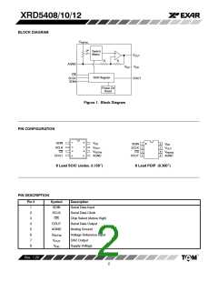
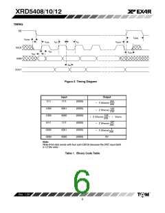
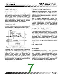
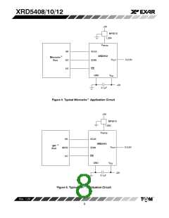
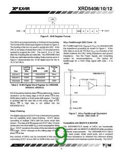
XRD5408/10/12
ELECTRICAL CHARACTERISTICS (CONT’D)
Test Conditions: V = 5V, GND= 0V, REFIN= 2.048V (External), R = 10kΩ, C = 100pF, T = T
to T
,
MAX
DD
L
L
A
MIN
Unless Otherwise Noted.
Symbol Parameter
Min.
Typ.
Max.
Unit
Conditions
Voltage Output (VOUT) XRD5408/10/12
V
--0.4
VO
VREG
+ISC
-ISC
Output Voltage Range
0
V
DD
Output Load Regulation
Short-Circuit Current, Sink
Short-Circuit Current, Source
2
13
7
4
mV
mA
mA
VOUT = 2V, RL=2kΩ
VOUT = VDD
VOUT = GND
Voltage Reference Input (VREFIN) XRD5408/10/12
Output Swing Limited, Not Code Dependent
VREFIN
RIN
Voltage Range
0
VDD
V
Input Resistance
Input Resistance Tempco
Input Capacitance
AC Feedthrough
40
65
1500
32
kΩ
TCRIN
CIN
ppm/°C
pF
40
Not Code Dependent
ACFT
-80
dB
REFIN = 1kHz, 2Vp-p, SDIN=000h
Digital Inputs (SDIN, SCLK, CS) XRD5408/10/12
VIH
VIL
IIN
Input High
3.5
V
V
Input Low
1
Input Current
Input Capacitance
‵ 1
µA
pF
VIN=0V or VDD
CIN
10
Digital Output (DOUT) XRD5408/10/12
VOH
VOL
Output High
Output Low
VDD-1
0.13
V
V
ISOURCE=4mA
ISINK=4mA
0.4
15
Dynamic Performance XRD5408/10/12
SR
ts
Voltage-Output Slew Rate
Voltage-Output Settling Time
Digital Feedthrough
0.21
13
1
V/µs
µs
TA=+25°C
‵ 1/2LSB, VOUT=2V
CS=VDD, SDIN=SCLK=100kHz
DFT
nV-s
dB
SINAD
Signal-to-Noise Plus Distortion
68
VREFIN=1kHz, 2Vp-p F.S., SDIN=Full
Scale, --3dB BW=250kHz
Power Supply XRD5408/10/12
VDD
IDD
Positive Supply Voltage
Power Supply Current
4.5
5.5
60
V
35
20
µA
All Inputs=0V or VDD, Output=No Load,
IREF Not Included, VO=0V (Note 1
)
Switching Characteristics XRD5408/10/12
tCSS
tCSH0
tCSH1
tCH
CS Setup Time
10
5
ns
ns
ns
ns
ns
SCLK Fall to CS Fall Hold Time
SCLK Fall to CS Rise Hold TIme
SCLK High Width
0
20
20
35
35
tCL
SCLK Low Width
Notes:
1 Total supply current consumption = IDD + IREF + (VO / 70K.)
Rev. 1.20
4

 EXAR [ EXAR CORPORATION ]