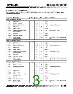
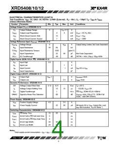
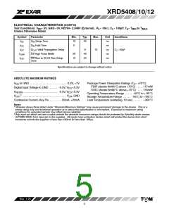
XRD5408/10/12
THEORY OF OPERATION
XRD5408/10/12 Description
Fixed Gain +2 Voltage Output Amplifier
A high open-loop gain operational amplifier buffers the
resistor string with a stable, fixed gain of +2. The voltage
output will settle within 13 s. The output is short circuit
protected and can regulate an output load of 2V into 2k
within 2mV at 25°C.
The XRD5408/10/12 are micro-power, voltage output,
serial daisy-chain programmable DACs operating from a
single 5V power supply. The DACs are built on a 0.6
micron CMOS process. The features of these DACs
make it well suited for industrial control, low distortion
audio, battery operated devices and cost sensitive
designs that want to minimize pin count on ICs.
While the reference input will accept a voltage from
rail-to-rail, the linear input voltage range is constrained by
the output swing of the fixed +2 closed-loop gain amplifier.
Full scale output swing is achieved with an external
reference of approximately 1/2 V
voltage must be positive because the XRD5408/10/12
DAC is non-inverting.
.
The reference
DD
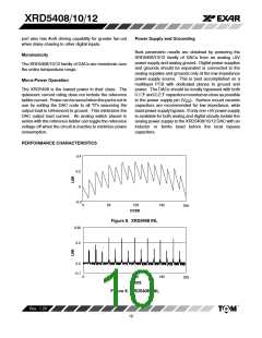
Resistor String DAC
A resistor string architecture converts digital data using a
switch matrix to an analog signal as shown in Figure 3.
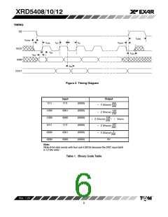
Serial Daisy-Chainable Digital Interface
V
REFIN
The three wire serial interface includes a DOUT to enable
daisy-chaining of several DACs. This minimizes pin
count necessary of digital asics or controllers to address
multiple DACS. The serial interface is designed for
CMOS logic levels. Timing is shown in Figure 2. The
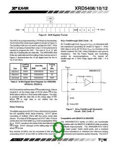
binary coding table (Table 1) shows the DAC transfer
function.
n
2
Switch
Matrix
+
-
V
OUT
R
R
AGND
V
V
DD
DD
CS
SCLK
SDIN
Shift Register
DOUT
A power on reset circuit forces the DAC to reset to all “0”s
on power up.
Power On
Reset
APPLICATION NOTES
Serial Interface
Figure 3. XRD5408/10/12 DAC Architecture
The resistor string architecture provides a non-inverted
output voltage (V
) of the reference input (V
) for
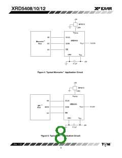
The XRD5408/10/12 family has a three wire serial
interface that is compatible with Microwiret, SPIt and
QSPIt standards. Typical configurations are shown in
Figure 4 and Figure 5. Maximum serial port clock rate is
OUT
REFIN
single supply operation while maintaininga constant input
resistance. Unlike inverted R-2R architectures the
reference input resistance will remain constant
independent of code. This greatly simplifies the analog
driving source requirements for the reference voltage and
minimizes distortion. Similarly input capacitance varies
only approximately 4pF over all codes.
limited by the minimum pulse width of t
and t .
CL
CH
Feedthrough noise from the serial port to the analog
output (V ) is minimized by lowering the frequency of
OUT
the serial port and holding the digital edges to >5ns.
Rev. 1.20
7

 EXAR [ EXAR CORPORATION ]