PDF
最近搜索
热门搜索
发布采购

| 型号: | XRD5408AIP |
| PDF下载: | 下载PDF文件 查看货源 |
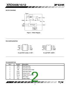
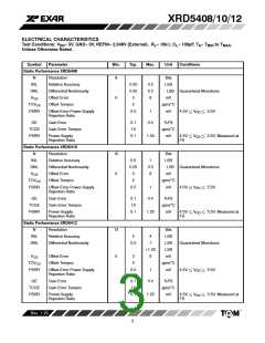
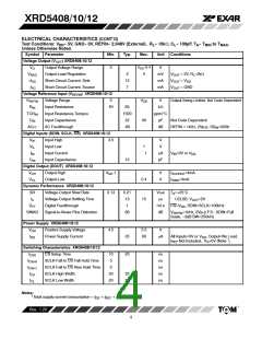
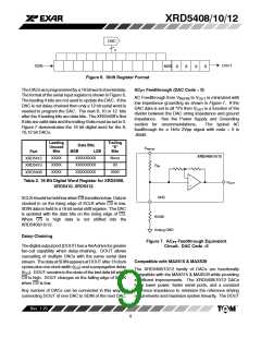
| 内容描述: | 5V ,低功耗,电压输出串行8月10日/ 12-位DAC系列 [5V, Low Power, Voltage Output Serial 8/10/12-Bit DAC Family] |
| 分类和应用: | 转换器数模转换器光电二极管 |
| 文件页数/大小: | 16 页 / 929 K |
| 品牌: |  EXAR [ EXAR CORPORATION ] EXAR [ EXAR CORPORATION ] |
专业IC领域供求交易平台:提供全面的IC Datasheet资料和资讯,Datasheet 1000万数据,IC品牌1000多家。