ST16C650A
2.90V TO 5.5V UART WITH 32-BYTE FIFO
áç
REV. 5.0.0
40-
44-
48-
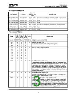
NAME
PDIP PLCC TQFP TYPE
DESCRIPTION
PIN #
38
PIN #
42
PIN #
40
CD#
RI#
I
I
Carrier Detect input or general purpose input (active low)
Ring Indicator input or general purpose input (active low)
39
43
41
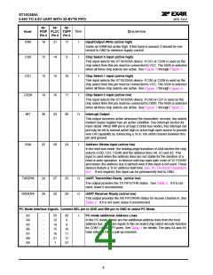
ANCILLARY SIGNALS
XTAL1
XTAL2
RCLK
16
17
9
18
19
10
14
15
5
I
O
I
Crystal or external clock input. Caution: this input is not 5V tolerant.
Crystal or buffered clock output
Receiver Clock
This input is used as external 16X clock input to the receiver section. Con-
nect the BAUDOUT# pin to this input externally.
BAUDOUT#
15
17
12
O
Baud Rate Generator Output (active low)
This pin provides the 16X clock of the selected data rate from the baud
rate generator. The RCLK pin must be connected externally to BAUD-
OUT# when the receiver is operating at the same data rate.
When the PC mode is selected, the baud rate generator clock output is
internally connected to the RCLK input. This pin then functions as the
LPT-1 printer port decode logic output, see Table 3.
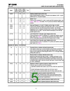
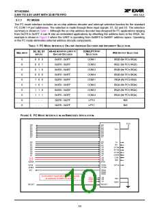
SEL
-
34
26
39
36
22
35
I
O
I
PC Mode Select (active low)
When this input is at logic 0, it enables the on-board chip select decode
function according to PC ISA bus COM[4:1] and IRQ[4:3] port definitions.
See Table 3 for details. This pin has an internal 100kΩ pull-up resistor.
DDIS#
RESET
23
35
Drive Disable Output
This pin goes to a logic 0 whenever the host CPU is reading data from the
650A. It can control the direction of a data bus transceiver between the
CPU and 650A or other logic functions.
Reset Input (active high)
A 40 ns minimum active pulse on this pin will reset the internal registers
and all outputs. The UART transmitter output will be held at logic 1, the
receiver input will be ignored and outputs are reset. See UART Reset
Conditions in Table 13.
OP1#
OP2#
VCC
34
31
40
38
35
44
34
31
42
O
O
Output Port 1
General purpose output.
Output Port 2
General purpose output.
Pwr 2.90V to 5.5V supply voltage
All inputs are 5V tolerant except for XTAL for devices with date code top
mark of "HC YYWW" and newer. Devices with date code top mark of "GC
YYWW" and older do not have 5V tolerant inputs.
GND
NC
20
-
22
-
18
Pwr Power supply common ground
1, 13,
25
-
No Connect
Pin type: I=Input, O=Output, IO= Input/output, OD=Output Open Drain.
6

 EXAR [ EXAR CORPORATION ]