ST16C650A
2.90V TO 5.5V UART WITH 32-BYTE FIFO
áç
REV. 5.0.0
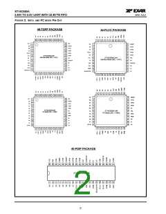
40-
44-
48-
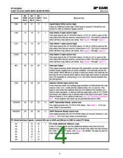
NAME
PDIP PLCC TQFP TYPE
DESCRIPTION
PIN #
PIN #
PIN #
IOW
19
21
17
I
I
Input/Output Write (active high)
Same as IOW# but active high. If this input is unused, it should be con-
nected to GND to minimize supply current.
CS0
CS1
CS2#
INT
12
13
14
30
14
15
16
33
9
Chip Select 0 input (active high)
This input selects the ST16C650A device. If CS1 or CS2# is used as the
chip select then this pin must be connected to VCC. The 650A is selected
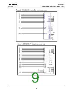
when all three chip selects are active. See Figure 3 through Figure 5.
10
11
30
I
I
Chip Select 1 input (active high)
This input selects the ST16C650A device. If CS0 or CS2# is used as the
chip select then this pin must be connected to VCC. The 650A is selected
when all three chip selects are active. See Figure 3 through Figure 5.
Chip Select 2 input (active low)
This input selects the ST16C650A device. If CS0 or CS1 is used as the
chip select then this pin must be connected to GND. The 650A is selected
when all three chip selects are active. See Figure 3 through Figure 5.
O
Interrupt Output
This output becomes active whenever the transmitter, receiver, line and/or
modem status register has an active condition. See interrupt section for
more detail. When IM# pin is at logic 0 (Intel bus mode), this interrupt out-
put may be set to normal active high or active high open source to provide
wire-OR capability by connecting a 1k to 10k ohms resistor between this
pin and ground.
AS#
25
28
24
I
Address Strobe input (active low)
In the Intel bus mode, the leading-edge transition of AS# latches the chip
selects (CS0, CS1, CS2#) and the address lines A0, A1 and A2. This
input is used when the address lines are not stable for the duration of a
read or write operation. In devices with top mark date code of "I2 YYWW"
and newer, the address bus is latched even if this input is not used. These
devices feature a ’0 ns’ address hold time. See “AC Electrical Characteris-
tics” . If not required, this input can be permanently tied to GND.
TXRDY#
RXRDY#
24
29
27
32
23
29
O
O
UART Transmitter Ready (active low)
The output provides the TX FIFO/THR status. See Table 2. If it is not
used, leave it unconnected.
UART Receiver Ready (active low)
This output provides the RX FIFO/RHR status for receive channel A. See
Table 2. If it is not used, leave it unconnected.
PC Mode Interface Signals. Connect SEL pin to GND and IM# pin to GND to select PC Mode.
A3
A4
A5
A6
A7
A8
A9
-
-
-
-
-
-
-
25
12
14
15
16
21
1
20
6
I
PC mode additional Address Lines
In the PC mode, these are the additional address lines from the host
address bus. They are inputs to the on-board chip select decode function
for COM 1-4 and LPT ports. See Table 1 for details. The pins A4 and A9
have internal 100kΩ pull-up resistors.
9
10
11
17
37
4

 EXAR [ EXAR CORPORATION ]