áç
ST16C650A
2.90V TO 5.5V UART WITH 32-BYTE FIFO
REV. 5.0.0
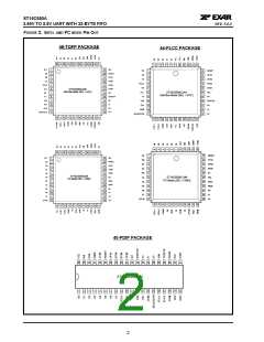
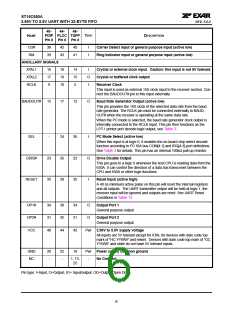
ORDERING INFORMATION
OPERATING
TEMPERATURE
RANGE
PART NUMBER
PACKAGE
DEVICE STATUS
ST16C650ACP40
ST16C650ACJ44
ST16C650ACQ48
ST16C650AIP40
ST16C650AIJ44
ST16C650AIQ48
40-Lead PDIP
44-Lead PLCC
48-Lead TQFP
40-Lead PDIP
44-Lead PLCC
48-Lead TQFP
0°C to +70°C Discontinued. See the ST16C650ACQ48 for a replacement.
0°C to +70°C Active
0°C to +70°C Active
-40°C to +85°C Discontinued. See the ST16C650AIQ48 for a replacement.
-40°C to +85°C Active
-40°C to +85°C Active
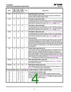
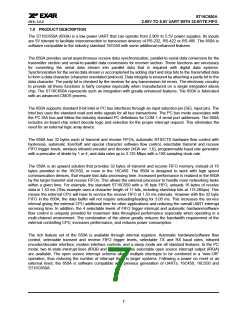
PIN DESCRIPTIONS
40-
PDIP PLCC TQFP TYPE
PIN # PIN # PIN #
44-
48-
NAME
DESCRIPTION
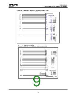
16 (Intel) MODE DATA BUS INTERFACE. The SEL pin is connected to VCC.
A2
A1
A0
26
27
28
29
30
31
26
27
28
I
Address bus lines [2:0]
A2:A0 selects internal UART’s configuration registers.
D7
D6
D5
D4
D3
D2
D1
D0
8
7
6
5
4
3
2
1
9
8
7
6
5
4
3
2
4
IO
Data bus lines [7:0] (bidirectional)
3
2
47
46
45
44
43
IOR#
21
24
19
I
Input/Output Read (active low)
The falling edge instigates an internal read cycle and retrieves the data
byte from an internal register pointed by the address lines [A2:A0], places
it on the data bus to allow the host processor to read it on the leading
edge. Its function is the same as IOR, except it is active low. Either an
active IOR# or IOR is required to transfer data from 650A to CPU during a
read operation. If this input is unused, it should be connected to VCC to
minimize supply current.
IOR
22
18
25
20
20
16
I
I
Input/Output Read (active high)
Same as IOR# but active high. If this input is unused, it should be con-
nected to GND to minimize supply current.
IOW#
Input/Output Write (active low) - Intel bus mode
The falling edge instigates the internal write cycle and the trailing edge
transfers the data byte on the data bus to an internal register pointed by
the address lines [A2:A0]. Its function is the same as IOW, except it is
active low. Either an active IOW# or IOW is required to transfer data from
650A to the Intel type CPU during a write operation. If this input is unused,
it should be connected to VCC to minimize supply current.
3

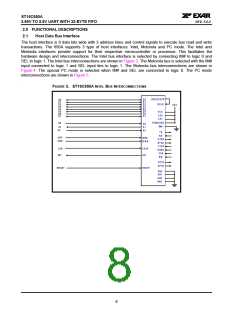
 EXAR [ EXAR CORPORATION ]