ST16C580
GENERAL DESCRIPTION
encoder/decoderinterface,modeminterfacecontrols,
andasleepmodeareallstandardfeatures.Followinga
poweronresetoranexternalreset,the580issoftware
compatiblewithpreviousgenerationofUARTs,16C450
and16C550.
The 580 provides serial asynchronous receive data
synchronization, parallel-to-serial and serial-to-paral-
lel data conversions for both the transmitter and
receiver sections. These functions are necessary for
convertingtheserialdatastreamintoparalleldatathat
is required with digital data systems. Synchronization
for the serial data stream is accomplished by adding
start and stops bits to the transmit data to form a data
character (character orientated protocol). Data integ-
rity is insured by attaching a parity bit to the data
character. The parity bit is checked by the receiver for
any transmission bit errors. The electronic circuitry to
provide all these functions is fairly complex especially
when manufactured on a single integrated silicon
chip. The ST16C580 represents such an integration
with greatly enhanced features. The 580 is fabricated
with an advanced CMOS process.
FUNCTIONAL DESCRIPTIONS
Internal Registers
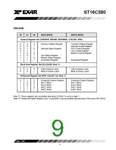
The 580 provides 15 internal registers for monitoring
andcontrol.TheseregistersareshowninTable3below.
Twelveregistersaresimilartothosealreadyavailablein
thestandard16C550.Theseregistersfunctionasdata
holdingregisters(THR/RHR),interruptstatusandcon-
trol registers (IER/ISR), a FIFO control register (FCR),
line status and control registers, (LCR/LSR), modem
status and control registers (MCR/MSR), program-
mable data rate (clock) control registers (DLL/DLM),
and a user assessable scratchpad register (SPR).
Beyond the general 16C550 features and capabilities,
the 580 offers an enhanced feature register set (EFR,
Xon/Xoff1-2)thatprovidesonboardhardware/software
flowcontrol.Registerfunctionsaremorefullydescribed
inthefollowingparagraphs.
The 580 is an upward solution that provides 16 bytes
of transmit and receive FIFO memory, instead of 16
bytes provided in the 16C550, or none in the 16C450.
The 580 is designed to work with high speed modems
and shared network environments, that require fast
data processing time. Increased performance is real-
ized in the 580 by the larger transmit and receive
FIFO’s. This allows the external processor to handle
more networking tasks within a given time. In addition,
the 4 selectable levels of FIFO trigger interrupt and
automatic hardware/software flow control is uniquely
provided for maximum data throughput performance
especially when operating in a multi-channel environ-
ment. The combination of the above greatly reduces
the bandwidth requirement of the external controlling
CPU, increases performance, and reduces power
consumption.
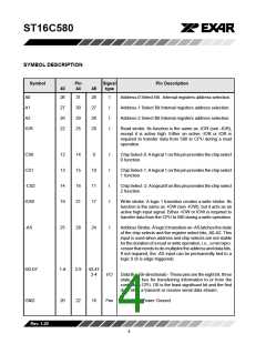
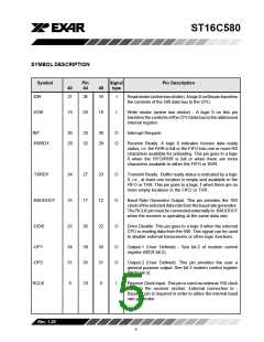
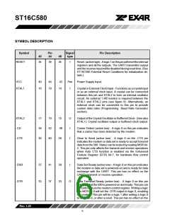
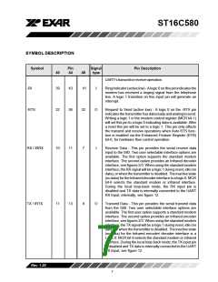
Table 3, INTERNAL REGISTER
The 580 is capable of operation to 1.5Mbps with a 24
MHz crystal or external clock input.
With a crystal of 7.3728 MHz and through a software
option, theusercanselectdataratesupto460.8Kbps.
The rich feature set of the 580 is available through
internal registers. Automatic hardware/software flow
control, selectable transmit and receive FIFO trigger
levels, selectable TX and RX baud rates, infrared
Rev.1.20
8

 EXAR [ EXAR CORPORATION ]