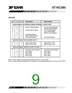
ST16C580
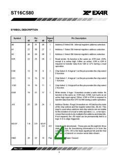
SYMBOL DESCRIPTION
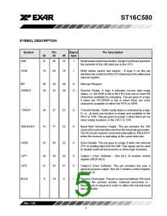
Symbol
Pin
44
Signal
type
Pin Description
40
48
-IOR
21
24
19
I
Readstrobe(activelowstrobe).Alogic0onthispintransfers
the contents of the 580 data bus to the CPU.
-IOW
18
20
16
I
Write strobe (active low strobe) - A logic 0 on this pin
transfers the contents of the CPU data bus to the addressed
internal register.
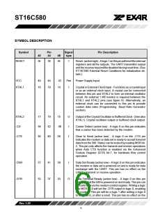
INT
30
29
33
32
30
29
O
O
Interrupt Request.
-RXRDY
Receive Ready. A logic 0 indicates receive data ready
status, i.e. the RHR is full or the FIFO has one or more RX
characters available for unloading. This pin goes to a logic
0 when the FIFO/RHR is full or when there are more
characters available in either the FIFO or RHR.
-TXRDY
-BAUDOUT
-DDIS
24
15
23
27
17
26
23
12
22
O
O
O
Transmit Ready. Buffer ready status is indicated by a logic
0, i.e., at least one location is empty and available in the
FIFO or THR. This pin goes to a logic 1 when there are no
more empty locations in the FIFO or THR.
Baud Rate Generator Output. This pin provides the 16X
clock of the selected data rate from the baud rate generator.
The RCLK pin must be connected externally to -BAUDOUT
when the receiver is operating at the same data rate.
Drive Disable. This pin goes to a logic 0 when the external
CPU is reading data from the 580. This signal can be used
to disable external transceivers or other logic functions.
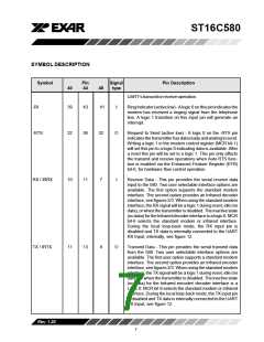
-OP1
-OP2
34
31
38
35
34
31
O
O
Output-1 (User Defined) - See bit-2 of modem control
register (MCR bit-2).
Output-2 (User Defined). This pin provides the user a
general purpose output. See bit-3 modem control register
(MCR bit-3).
RCLK
9
10
5
I
Receive Clock Input. This pin is used as external 16X clock
input to the receiver section. External connection to -
Baudout pin is required in order to utilize the internal baud
rate generator.
Rev.1.20
5

 EXAR [ EXAR CORPORATION ]