ST16C580
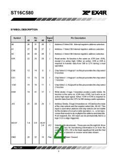
SYMBOL DESCRIPTION
Symbol
Pin
44
Signal
type
Pin Description
40
48
RESET
35
39
35
I
Reset.(activehigh)-Alogic1onthispinwillresettheinternal
registers and all the outputs. The UART transmitter output
andthereceiverinputwillbedisabledduringresettime.(See
ST16C580 External Reset Conditions for initialization de-
tails.)
VCC
40
16
44
18
42
Pwr
I
Power Supply Input.
XTAL1
14
Crystal or External Clock Input - Functions as a crystal input
or as an external clock input. A crystal can be connected
between this pin and XTAL2 to form an internal oscillator
circuit. An external 1 M resistor is required between the
XTAL1 and XTAL2 pins (see figure 9). Alternatively, an
external clock can be connected to this pin to provide
custom data rates (Programming Baud Rate Generator
section).
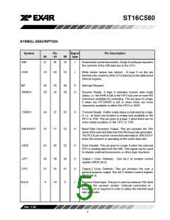
XTAL2
-CD
17
38
36
19
42
40
15
40
38
O
I
OutputoftheCrystalOscillatororBufferedClock-(Seealso
XTAL1). Crystal oscillator output or buffered clock output.
Carrier Detect (active low) - A logic 0 on this pin indicates
that a carrier has been detected by the modem.
-CTS
I
Clear to Send (active low) - A logic 0 on the -CTS pin
indicates the modem or data set is ready to accept transmit
data from the 580. Status can be tested by reading MSR bit-
4. This pin only affects the transmit and receive operations
when Auto CTS function is enabled via the Enhanced
Feature Register (EFR) bit-7, for hardware flow control
operation.
-DSR
-DTR
37
33
41
37
39
33
I
Data Set Ready (active low) - A logic 0 on this pin indicates
the modem or data set is powered-on and is ready for data
exchange with the UART. This pin has no effect on the
UART’s transmit or receive operation.
O
Data Terminal Ready (active low) - A logic 0 on this pin
indicatesthatthe580ispowered-onandready. Thispincan
be controlled via the modem control register. Writing a logic
1 to MCR bit-0 will set the -DTR output to logic 0, enabling
the modem. This pin will be a logic 1 after writing a logic 0
to MCR bit-0, or after a reset. This pin has no effect on the
Rev.1.20
6

 EXAR [ EXAR CORPORATION ]