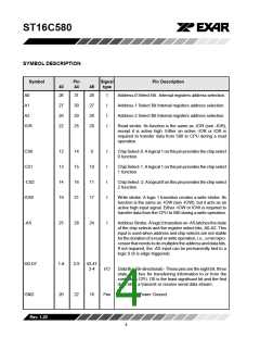
ST16C580
SYMBOL DESCRIPTION
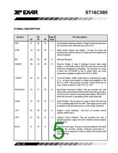
Symbol
Pin
44
Signal
type
Pin Description
40
48
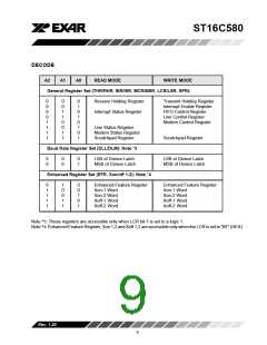
A0
28
31
30
29
25
28
I
I
I
I
Address-0 Select Bit - Internal registers address selection.
Address-1 Select Bit Internal registers address selection.
Address-2 Select Bit Internal registers address selection.
A1
27
26
22
27
26
20
A2
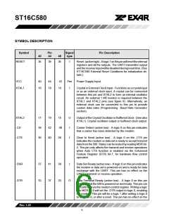
IOR
Read strobe. Its function is the same as -IOR (see -IOR),
except it is active high. Either an active -IOR or IOR is
required to transfer data from 580 to CPU during a read
operation.
CS0
CS1
-CS2
IOW
12
13
14
19
14
15
16
21
9
I
I
I
I
Chip Select-0. A logical 1 on this pin provides the chip select
0 function.
10
11
17
Chip Select-1. A logical 1 on this pin provides the chip select
1 function.
ChipSelect-2. Alogical0onthispinprovidesthechipselect
2 function.
Write strobe. A logic 1 transition creates a write strobe. Its
function is the same as -IOW (see -IOW), but it acts as an
active high input signal. Either -IOW or IOW is required to
transfer data from the CPU to 580 during a write operation.
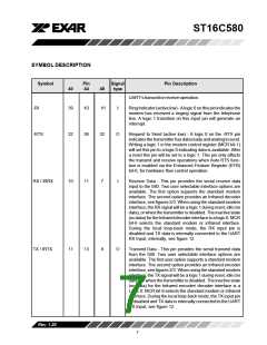
-AS
25
28
24
I
Address Strobe. A logic 0 transition on -AS latches the state
of the chip selects and the register select bits, A0-A2. This
input is used when address and chip selects are not stable
for the duration of a read or write operation, i.e., a micropro-
cessor that needs to de-multiplex the address and data bits.
If not required, the -AS input can be permanently tied to a
logic 0 (it is edge triggered).
D0-D7
GND
1-8
20
2-9
22
43-47
2-4
I/O
Data Bus (Bi-directional) - These pins are the eight bit, three
state data bus for transferring information to or from the
controlling CPU. D0 is the least significant bit and the first
data bit in a transmit or receive serial data stream.
18
Pwr
Signal and Power Ground.
Rev.1.20
4

 EXAR [ EXAR CORPORATION ]