ABSOLUTE MAXIMUM RATINGS
These are stress ratings only and functional operation
of the device at these ratings or any other above those
indicated in the operation sections of the specifications
below is not implied. Exposure to absolute maximum
rating conditions for extended periods of time may
affect reliability.
Output Voltages
Logic.........................-0.3V to (Vcc + 0.5V)
Drivers.............................................+/-15V
Receivers..................-0.3V to (Vcc + 0.5V)
Storage Temperature.......................-65˚C to +150˚C
Power Dissipation
8-pin NSOIC...................................................550mW
(derate 6.60mW/ºC above +70ºC)
8-pin PDIP....................................................ꢀ000mW
(derate ꢀꢀ.8mW/ºC above +70ºC)
VCC.......................................................................+7V
Input Voltages
Logic.........................-0.3V to (Vcc + 0.5V)
Drivers......................-0.3V to (Vcc + 0.5V)
Receivers.........................................+/-15V
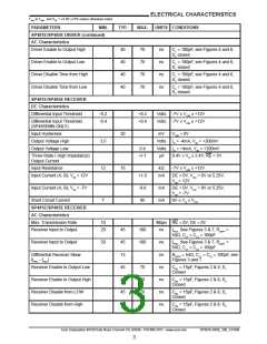
ELECTRICAL CHARACTERISTICS
TMIN to TMAX and VCC = +5.0V +/-5% unless otherwise noted.
PARAMETERS
MIN.
TYP.
MAX.
UNITS CONDITIONS
SP481E/SP485E DRIVER
DC Characteristics
Differential Output Voltage
Differential Output Voltage
GND
2
Vcc
Vcc
Volts
Volts
Unloaded; R = ∞ ; see Figure 1
With Load; R = 50Ω (RS-422); see
Figure 1
Differential Output Voltage
ꢀ.5
2.0
Vcc
0.2
Volts
Volts
With Load; R = 27Ω (RS-485); see
Figure 1
Change in Magnitude of Driver
Differential Output Voltage for
Complimentary states
R = 27Ω or R = 50Ω; see Figure 1
Driver Common Mode Output
Voltage
3
Volts
R = 27Ω or R = 50Ω; see Figure 1
Input High Voltage
Input Low Voltage
Input Current
Volts
Volts
µA
Applies to DE, DI, RE
Applies to DE, DI, RE
Applies to DE, DI, RE
0.8
+/-ꢀ0
Driver Short Circuit Current
VOUT = HIGH
+/-250
+/-250
mA
mA
-7V ≤ VO ≤ +12V
-7V ≤ VO ≤ +12V
VOUT = LOW
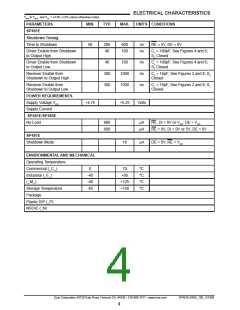
SP481E/SP485E DRIVER
AC Characteristics
Max. Transmission Rate
ꢀ0
Mbps
RE = 5V, DE = 5V; RDIFF = 54Ω,
CLꢀ = CL2 = ꢀ00pF
Driver Input to Output, tPLH
20
20
30
30
60
80
ns
ns
See Figures 3 & 5, RDIFF = 54Ω,
CLꢀ = CL2 = ꢀ00pF
Driver Input to Output, tPLH
(SP485EMN ONLY)
Driver Input to Output, tPHL
20
20
30
30
60
80
ns
ns
See Figures 3 & 5, RDIFF = 54Ω,
CLꢀ = CL2 = ꢀ00pF
Driver Input to Output, tPHL
(SP485EMN ONLY)
Driver Skew
5
ꢀ0
40
ns
ns
see Figures 3 and 5,
tSKEW = |tDPHL - tDPLH
|
Driver Rise or Fall Time
3
ꢀ5
From ꢀ0%-90%; RDIFF = 54Ω
CLꢀ = CL2 = 100pF; see Figures 3
and 6
Exar Corporation 48720 Kato Road, Fremont CA, 94538 • 5ꢀ0-668-70ꢀ7 • www.exar.com
SP48ꢀE,485E_ꢀ00_ꢀ2ꢀ808
2

 EXAR [ EXAR CORPORATION ]