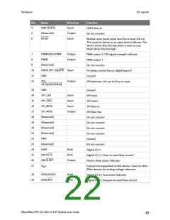
Hardware
Design notes
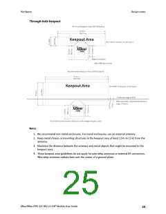
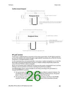
Surface-mount keepout
RF pad version
The RF pad is a soldered antenna connection on the surface-mount device. The RF signal travels from
pin 36 on the module to the antenna through a single ended RF transmission line on the PCB. This line
should have a controlled impedance of 50 Ω.
For the transmission line, we recommend either a microstrip or coplanar waveguide trace on the PCB.
We provide a microstrip example below, because it is simpler to design and generally requires less
area on the host PCB than coplanar waveguide.
We do not recommend using a stripline RF trace because that requires routing the RF trace to an inner
PCB layer, and via transitions can introduce matching and performance problems.
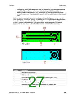
The following figure shows a layout example of a microstrip connecting an RF pad module to a
through-hole RPSMA RF connector.
n
The top two layers of the PCB have a controlled thickness dielectric material in between. The
second layer has a ground plane which runs underneath the entire RF pad area. This ground
plane is a distance d, the thickness of the dielectric, below the top layer.
n
The top layer has an RF trace running from pin 36 of the device to the RF pin of the RPSMA
connector. The RF trace's width determines the impedance of the transmission line with
XBee/XBee-PRO S2C 802.15.4 RF Module User Guide
26

 ETC [ ETC ]