Hardware
Design notes
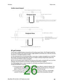
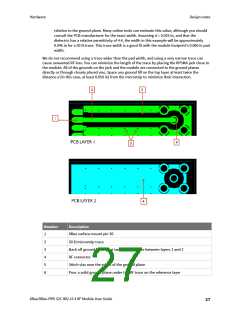
relation to the ground plane. Many online tools can estimate this value, although you should
consult the PCB manufacturer for the exact width. Assuming d = 0.025 in, and that the
dielectric has a relative permittivity of 4.4, the width in this example will be approximately
0.045 in for a 50 Ω trace. This trace width is a good fit with the module footprint's 0.060 in pad
width.
We do not recommend using a trace wider than the pad width, and using a very narrow trace can
cause unwanted RF loss. You can minimize the length of the trace by placing the RPSMA jack close to
the module. All of the grounds on the jack and the module are connected to the ground planes
directly or through closely placed vias. Space any ground fill on the top layer at least twice the
distance d (in this case, at least 0.050 in) from the microstrip to minimize their interaction.
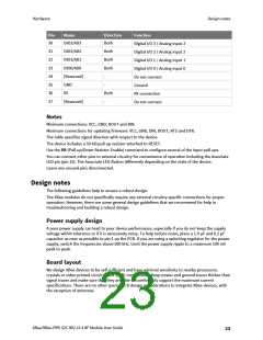
Number
Description
XBee surface-mount pin 36
1
2
3
4
5
6
50 Ω microstrip trace
Back off ground fill at least twice the distance between layers 1 and 2
RF connector
Stitch vias near the edges of the ground plane
Pour a solid ground plane under the RF trace on the reference layer
XBee/XBee-PRO S2C 802.15.4 RF Module User Guide
27

 ETC [ ETC ]