Hardware
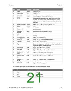
Pin signals
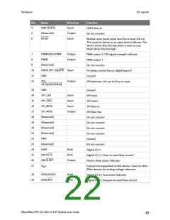
Pin
Name
Direction
Function
4
5
6
DIN/CONFIG
Input
UART data in
Do not connect
[Reserved]
RESET
Output
Input
Module reset (reset pulse must be at least 200 ns).
This must be driven as an open drain/collector. The
device drives this line low when a reset occurs.
Never drive this line high.
7
PWM0/RSSI PWM
PWM1
Output
Output
-
PWM output 0 / RX signal strength indicator
PWM output 1
8
9
[Reserved]
Do not connect
10
11
12
DI8/SLEEP_RQ/DTR Input
Pin sleep control line or digital input 8
Ground
GND
-
SPI_
Output
SPI Attention. Do not tie low on reset.
ATTN/BOOTMODE
13
14
15
16
17
18
19
20
21
22
23
24
25
26
27
GND
-
Ground
SPI_CLK
SPI_SSEL
SPI_MOSI
SPI_MISO
[Reserved]
[Reserved]
[Reserved]
[Reserved]
GND
Input
SPI clock
Input
SPI select
Input
SPI Data In
Output
SPI Data Out
-
Do not connect
Do not connect
Do not connect
Do not connect
Ground
-
-
-
-
[Reserved]
DIO4
-
Do not connect
Digital I/O 4
Both
Both
Output
-
DIO7/CTS
ON/SLEEP
Digital I/O 7 / Clear-to-send flow control
Device sleep status indicator
V
Feature not supported on this device. Used on other
XBee devices for analog voltage reference.
REF
28
29
DIO5/ASSOC
DIO6/RTS
Both
Both
Digital I/O 5 / Associated indicator
Digital I/O 6 / Request-to-send flow control
XBee/XBee-PRO S2C 802.15.4 RF Module User Guide
22

 ETC [ ETC ]