TLV9001, TLV9002, TLV9004
www.ti.com
SBOS833A –OCTOBER 2017–REVISED DECEMBER 2017
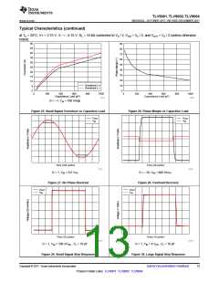
Typical Characteristics (continued)
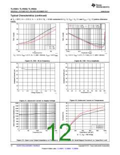
at TA = 25°C, V+ = 2.75 V, V– = –2.75 V, RL = 10 kΩ connected to VS / 2, VCM = VS / 2, and VOUT = VS / 2 (unless otherwise
noted)
50
45
40
35
30
25
20
15
10
5
90
80
70
60
50
40
30
20
10
0
Overshoot (+)
Overshoot (–)
0
0
200
400 600
Capacitance Load (pF)
800
1000
0
200
400
600
800
1000
Capacitance Load (pF)
D025
D026
G = –1, VIN = 100 mVpp
Figure 25. Small Signal Overshoot vs Capacitive Load
Figure 26. Phase Margin vs Capacitive Load
VOUT
VIN
VOUT
VIN
Time (100 ms/div)
Time (20 ms/div)
D027
D028
G = 1, VIN = 6.5 VPP
G = –10, VIN = 600 mVPP
Figure 27. No Phase Reversal
Figure 28. Overload Recovery
VOUT
VIN
VOUT
VIN
Time (10 ms/div)
Time (10 ms/div)
D029
D030
G = 1, VIN = 100 mVPP , CL = 10 pF
G = 1, VIN = 4 VPP , CL = 10 pF
Figure 29. Small-Signal Step Response
Figure 30. Large-Signal Step Response
Copyright © 2017, Texas Instruments Incorporated
Submit Documentation Feedback
13
Product Folder Links: TLV9001 TLV9002 TLV9004

 ETC [ ETC ]