Epson Research and Development
Page 9
Vancouver Design Center
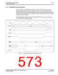
2.1.2 LCD Memory Access Cycles
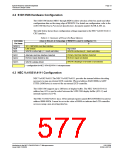
Once an address in the LCD block of memory is placed on the external address bus
(ADD[25:0]), the LCD chip select (LCDCS#) is driven low. The read or write enable
signals (RD# or WR#) are driven low for the appropriate cycle and LCDRDY is driven low
to insert wait states into the cycle. The high byte enable (SHB#) in conjunction with address
bit 0 allows for byte steering.
The following figure illustrates typical NEC VR4102/VR4111 memory read and write
cycles to the LCD controller interface.
TCLK
ADD[25:0]
VALID
SHB#
LCDCS#
WR#,RD#
D[15:0]
(write)
VALID
Hi-Z
D[15:0]
(read)
Hi-Z
VALID
LCDRDY
Figure 2-1: NEC VR4102/VR4111 Read/Write Cycles
Interfacing to the NEC VR4102/VR4111™ Microprocessors
S1D13506
Issue Date: 01/02/08
X25B-G-007-02

 EPSON [ EPSON COMPANY ]