Epson Research and Development
Page 11
Vancouver Design Center
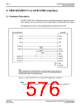
3.2 Host Bus Interface Signal Descriptions
The S1D13506 MIPS/ISA Host Bus Interface requires the following signals.
• BUSCLK is a clock input which is required by the S1D13506 Host Bus Interface. It is
separate from the input clock (CLKI) and is typically driven by the host CPU system
clock.
• The address inputs AB[20:0], and the data bus DB[15:0], connect directly to the
VR4102/VR4111 address (ADD[20:0]) and data bus (DAT[15:0]), respectively. MD4
must be set to select the proper endian mode upon reset.
• M/R# (memory/register) selects between memory or register access. It may be
connected to an address line, allowing system address ADD21 to be connected to the
M/R# line.
• Chip Select (CS#) must be driven low by LCDCS# whenever the S1D13506 is accessed
by the VR4102/VR4111.
• WE1# connects to SHB# (the high byte enable signal from the VR4102/VR4111) which
in conjunction with address bit 0 allows byte steering of read and write operations.
• WE0# connects to WR# (the write enable signal from the VR4102/VR4111) and must
be driven low when the VR4102/VR4111 is writing data to the S1D13506.
• RD# connects to RD# (the read enable signal from the VR4102/VR4111) and must be
driven low when the VR4102/VR4111 is reading data from the S1D13506.
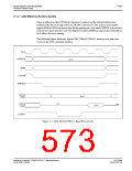
• WAIT# connects to LCDRDY and is a signal output from the S1D13506 that indicates
the VR4102/VR4111 must wait until data is ready (read cycle) or accepted (write cycle)
on the host bus. Since VR4102/VR4111 accesses to the S1D13506 may occur asynchro-
nously to the display update, it is possible that contention may occur in accessing the
S1D13506 internal registers and/or display buffer. The WAIT# line resolves these
contentions by forcing the host to wait until the resource arbitration is complete.
• The BS# and RD/WR# signals are not used for the MIPS/ISA Host Bus Interface and
should be tied high (connected to V ).
DD
Interfacing to the NEC VR4102/VR4111™ Microprocessors
Issue Date: 01/02/08
S1D13506
X25B-G-007-02

 EPSON [ EPSON COMPANY ]