Epson Research and Development
Page 5
Vancouver Design Center
List of Tables
Table 3-1: Host Bus Interface Pin Mapping . . . . . . . . . . . . . . . . . . . . . . . . . . . . . . 10
Table 4-1: Summary of Power-On/Reset Options . . . . . . . . . . . . . . . . . . . . . . . . . . . 13
List of Figures
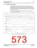
Figure 2-1: NEC VR4102/VR4111 Read/Write Cycles . . . . . . . . . . . . . . . . . . . . . . . . 9
Figure 4-1: NEC VR4102/VR4111 to S1D13506 Configuration Schematic . . . . . . . . . . . . . . 12
Interfacing to the NEC VR4102/VR4111™ Microprocessors
S1D13506
Issue Date: 01/02/08
X25B-G-007-02

 EPSON [ EPSON COMPANY ]