Page 12
Epson Research and Development
Vancouver Design Center
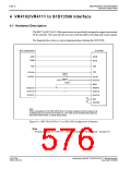
4 VR4102/VR4111 to S1D13506 Interface
4.1 Hardware Description
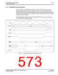
The NEC VR4102/VR4111 Microprocessors are specifically designed to support an external
LCD controller. They provide the necessary internal address decoding and control signals.
The diagram below shows a typical implementation utilizing the S1D13506.
NEC VR4102/VR4111
S1D13506
WR#
WE0#
SHB#
WE1#
RD#
RD#
CS#
LCDCS#
LCDRDY
Pull-up
WAIT#
System RESET
RESET#
ADD21
M/R#
AB[20:0]
DB[15:0]
BUSCLK
ADD[25:0]
DAT[15:0]
BUSCLK
VDD
VDD
BS#
RD/WR#
Note:
When connecting the S1D13506 RESET# pin, the system designer should be aware of all
conditions that may reset the S1D13506 (e.g. CPU reset can be asserted during wake-up
from power-down modes, or during debug states).
Figure 4-1: NEC VR4102/VR4111 to S1D13506 Configuration Schematic
Note
For pin mapping see Table 3-1:, “Host Bus Interface Pin Mapping,” on page 10.
S1D13506
Interfacing to the NEC VR4102/VR4111™ Microprocessors
X25B-G-007-02
Issue Date: 01/02/08

 EPSON [ EPSON COMPANY ]