Page 12
Epson Research and Development
Vancouver Design Center
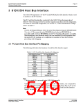
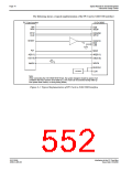
3.2 PC Card Host Bus Interface Signals
The S1D13506 PC Card Host Bus Interface is designed to support processors which
interface the S1D13506 through the PC Card bus.
The S1D13506 PC Card Host Bus Interface requires the following signals from the PC
Card bus.
• BUSCLK is a clock input which is required by the S1D13506 Host Bus Interface. It is
separate from the input clock (CLKI) and is typically driven by the host CPU system
clock. Since PC Card signalling is independent of any clock, BUSCLK can come from
any oscillator already implemented. For example, the source for the CLKI input of the
S1D13506 may be used.
• The address inputs AB[20:1], and the data bus DB[15:0], connect directly to the PC
Card address (A[20:1]) and data bus (D[15:0]), respectively. MD4 must be set to select
little endian mode upon reset.
• M/R# (memory/register) selects between memory or register access. It may be
connected to an address line, allowing system address A21 to be connected to the M/R#
line.
• Chip Select (CS#) must be driven low whenever the S1D13506 is accessed by the PC
Card bus.
• WE1# and RD/WR# connect to CE2# and CE1# (the byte enables for the high-order and
low-order bytes). They are driven low when the PC Card bus is accessing the
S1D13506.
• RD# connects to OE# (the read enable signal from the PC Card bus).
• WE0# connects to WE# (the write enable signal from the PC Card bus).
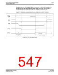
• WAIT# is a signal output from the S1D13506 that indicates the PC Card bus must wait
until data is ready (read cycle) or accepted (write cycle) on the host bus. Since PC Card
bus accesses to the S1D13506 may occur asynchronously to the display update, it is
possible that contention may occur in accessing the S1D13506 internal registers and/or
display buffer. The WAIT# line resolves these contentions by forcing the host to wait
until the resource arbitration is complete. For PC Card applications, this signal should
be set active low using the MD5 configuration input.
• The Bus Start (BS#) signal is not used for the PC Card Host Bus Interface and should be
tied high (connected to V ).
DD
• The RESET# (active low) input of the S1D13506 may be connected to the PC Card
RESET (active high) using an inverter.
S1D13506
X25B-G-005-03
Interfacing to the PC Card Bus
Issue Date: 01/02/06

 EPSON [ EPSON COMPANY ]