Epson Research and Development
Page 11
Vancouver Design Center
3 S1D13506 Host Bus Interface
The S1D13506 implements a 16-bit PC Card (PCMCIA) Host Bus Interface which is used
to interface to the PC Card bus.
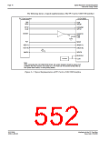
The PC Card Host Bus Interface is selected by the S1D13506 on the rising edge of
RESET#. After releasing reset the bus interface signals assume their selected configuration.
For details on S1D13506 configuration, see Section 4.2, “S1D13506 Hardware Configu-
ration” on page 15.
Note
At reset, the Register/Memory Select bit in the Miscellaneous Register (REG[001h] bit
7) is set to 1. This means that only REG[000h] (read-only) and REG[001h] are
accessible until a write to REG[001h] sets bit 7 to 0 making all registers accessible.
When debugging a new hardware design, this can sometimes give the appearance that
the interface is not working, so it is important to remember to clear this bit before
proceeding with debugging.
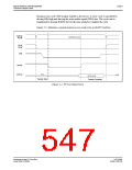
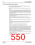
3.1 PC Card Host Bus Interface Pin Mapping
The following table shows the functions of each Host Bus Interface signal.
Table 3-1: PC Card Host Bus Interface Pin Mapping
S1D13506 Pin Name
AB[20:1]
DB[15:0]
WE1#
PC Card (PCMCIA)
A[20:1]1
D[15:0]
CE2#
M/R#
External Decode
External Decode
n/a2
CS#
BUSCLK
BS#
VDD
RD/WR#
RD#
CE1#
OE#
WE0#
WE#
WAIT#
WAIT#
RESET#
Inverted RESET
Note
1
The bus signal A0 is not used by the S1D13506 internally.
2
Although a clock is not directly supplied by the PC Card interface, one is required by
the S1D13506 PC Card Host Bus Interface. For an example of how this can be accom-
plished see the discussion on BUSCLK in Section 3.2, “PC Card Host Bus Interface
Signals” on page 12.
Interfacing to the PC Card Bus
Issue Date: 01/02/06
S1D13506
X25B-G-005-03

 EPSON [ EPSON COMPANY ]