Page 14
Epson Research and Development
Vancouver Design Center
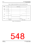
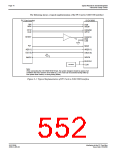
The following shows a typical implementation of the PC Card to S1D13506 interface.
PC Card socket
S1D13506
OE#
WE#
RD#
WE0#
CE1#
CE2#
RD/WR#
WE1#
RESET
RESET#
BS#
CS#
VDD
A21
M/R#
AB[20:1]
DB[15:0]
A[20:1]
D[15:0]
15K
WAIT#
WAIT#
BUSCLK
CLKI
Oscillator
Note:
When connecting the S1D13506 RESET# pin, the system designer should be aware of all
conditions that may reset the S1D13506 (e.g. CPU reset can be asserted during wake-up
from power-down modes, or during debug states).
Figure 4-1: Typical Implementation of PC Card to S1D13506 Interface
S1D13506
X25B-G-005-03
Interfacing to the PC Card Bus
Issue Date: 01/02/06

 EPSON [ EPSON COMPANY ]